Journal of Electromagnetic Analysis and Applications
Vol.4 No.5(2012), Article ID:19520,5 pages DOI:10.4236/jemaa.2012.45025
Optimal Design of Wideband Microwave Absorber Consisting of Resistive Meta-Surface Layers
![]()
1School of Electronic Science and Engineering, Nanjing University, Nanjing, China; 2College of Science, Nanjing University of Posts and Telecommunications, Nanjing, China.
Email: *yjfeng@nju.edu.cn
Received March 7th, 2012; revised April 9th, 2012; accepted April 20th, 2012
Keywords: Microwave Absorber; Meta-surface; Transmission Line Model; Genetic Algorithm
ABSTRACT
In this paper we propose an optimal design of ultra-wideband (4 ~ 20 GHz) microwave absorbers consisting of two resistive meta-surface layers of different square patch arrays. Gradient Descent and Genetic Algorithm numerical methods are employed to optimize all the parameters through equivalent transmission line circuit model. The circuit parameters are then implemented by a multilayer including two resistive meta-surfaces of square patch structures. Two types of such absorbing structures, with the total thicknesses close to that of the known theoretical limit, are designed and their performance are verified by full wave electromagnetic simulation.
1. Introduction
In recent years, increasing attention has been devoted to electromagnetic (EM) wave absorbers that exhibit excellent absorption properties in the microwave frequency band needed to solve the serious electromagnetic interference and compatibility problems in the rapid development of communications and radar systems. The most investigated and notable representatives of microwave absorber are the Salisbury Screen, Jauman absorber and circuit analogue absorber [1-4].
The Jauman absorber can be explained as a multilayer structure of Salisbury Screen [2,3]. Both of them can be classified as resistance screens. As we all know, Salisbury Screen is narrowband, while Jauman absorbers will broaden the absorbing bandwidth by sacrificing the thickness requirement.
Circuit analogue absorber, which is an improved version of Salisbury Screen, is often used to balance the conflicts between the total thickness and the bandwidth, and it has been proved to be a very useful method [4]. In recent years, resistance screens in Jauman or circuit analogue absorbers were often replaced by different shapes of artificial meta-surface or frequency selective surface (FSS) to realize a capacitive circuit absorber [5-8]. Strictly speaking, they should be still looked as improved resistance screen absorbers. However, in this way, two other parameters, the capacitance and inductance, can be introduced to optimize the absorbing bandwidth.
In the past few years, Ji-Chyun, etc. [5] proposed a hybrid metal grid/ferrite FSS screen structure to achieve microwave absorption of –10 dB over the X-band with a single layer. E. Yildirim, etc. [6] used a composition of two different shapes of FSS instead of a resistance layer to realize an absorption bandwidth from 11.5 GHz to 33 GHz. A. Kazemzaden, etc. [7] used a four-layer of different size of square patch to construct an absorption bandwidth from 3.16 ~ 34.96 GHz. Although these FSS structures can broaden the absorption bandwidth, they make the analysis process more complicated [8]. Furthermore, most of the analysis processes depend on empirical formulas, where some circuit parameters, such as the capacitance and inductance, cannot be acquired precisely.
In this paper, we combine Gradient Descent with Genetic Algorithm (GA) numerical method to optimize the multilayer absorbing structures including different metasurfaces through equivalent transmission line circuit model. Compared with the designs mentioned above, our optimal process is more simple and straightforward. Two examples of multilayer absorber are given to verify our optimal design by implementation of the optimal circuit parameters with different material and geometric parameters of the dielectric layers and meta-surfaces.
2. Design Objective
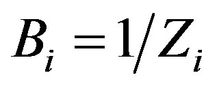
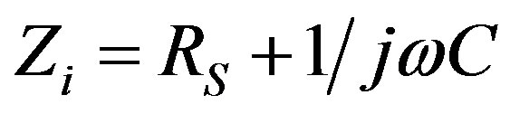
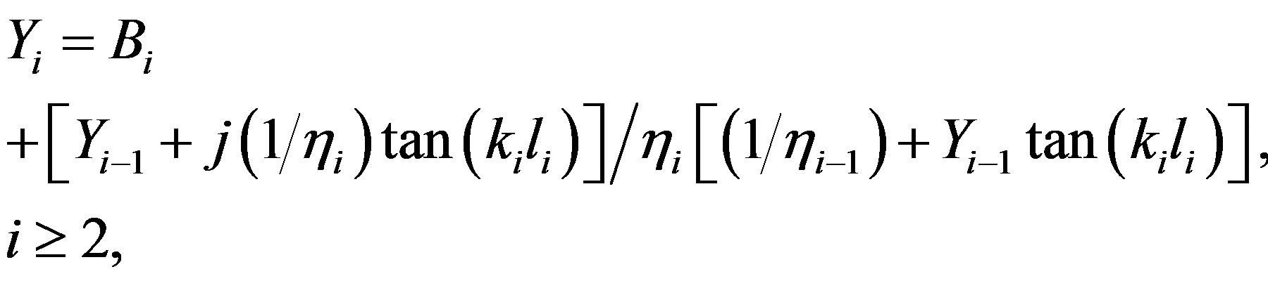
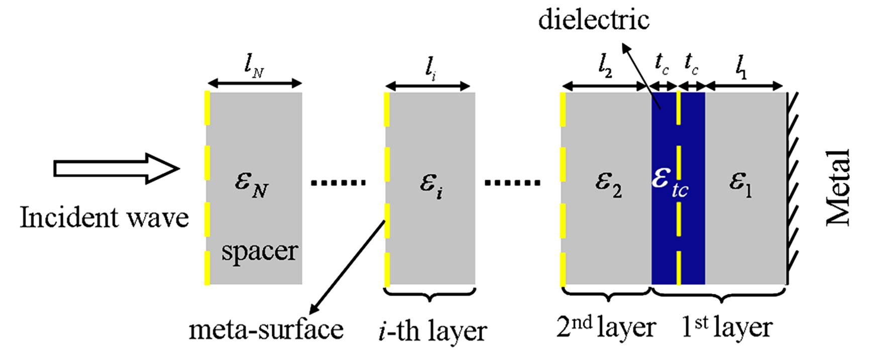
Firstly, we consider that the absorber is consisted of meta-surfaces spaced with dielectric media (see Figure 1(a)). The multilayer structure backed with a perfect conducting sheet can be explained by an equivalent transmission line circuit model shown in Figure 1(b). Here, we define Bi as the admittance of the i-th layer meta-surface, and Yi as the sum of the admittance of the i-th layer meta-surface and the i-th dielectric layer. They can be expressed as the following:
 , (1)
, (1)
 , (2)
, (2)
 , (3)
, (3)
 (4)
(4)
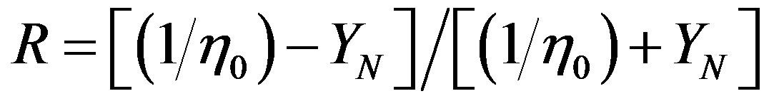
where Zi is the equivalent impedance of the i-th metasurface of patch array, C and RS represent the equivalent capacitance and the surface resistance of each patch, respectively. ηi denotes the wave impedance of the i-th layer medium, ki and li are the wave number and the depth of the i-th layer medium, respectively. Then, we have the reflection coefficient of such N-layered absorber,
 . (5)
. (5)
It has been found that, in the optimal design process, the influence of the capacitance value is much more important. In order to obtain a satisfied absorption effect in low frequency band, the capacitance of the first layer should be in the order of Pico Farad. Therefore, the first meta-surface layer is often embedded into another dielectric medium with high permittivity to increase the capacity [6], as indicated in the blue region of the 1st layer in Figure 1(a).
 (a)
(a)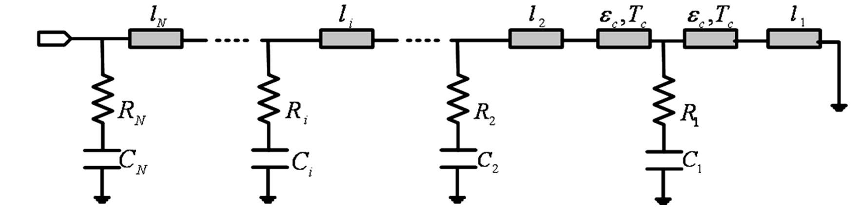 (b)
(b)
Figure 1. Schematic of multilayered absorber (a) and its corresponding transmission line circuit model (b).
Meta-surface with periodic patch arrays in the structure behave as band elimination filters. Generally speaking, the more periods in the structure, the better absorption effect it can reach. Our design objective is to construct ultra-wideband absorbers with least number of layers. Here, we will give a result of ultra-wideband multilayer absorber working from 4 GHz to 20 GHz with only two resistive meta-surface layers.
3. Optimization Process
In this section, we present the detailed optimization process for the two-layer ultra-wideband absorbers. The main problem can be summarized to a multi-dimensional multi-objective optimization for extreme value in mathematics. Assume that f is the function need to be optimized, which is the reflection coefficient in this problem; the objective function faim denotes the required reflection coefficient of the absorber over a certain frequency band. The total reflection coefficient depends on the frequency w and all the circuit parameters (xi), therefore the optimization is denoted as
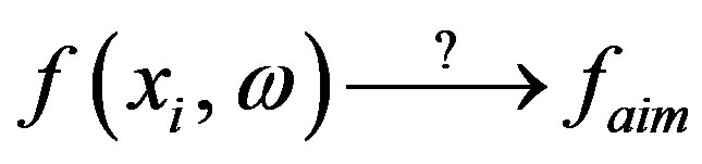 . (6)
. (6)
The initial points and the objective function determine the final results. Therefore, designers have to make selections according to the purpose of physics application.
In our optimization process, Gradient Descent is firstly used to find the minimum points quickly; then, GA is employed to get the final optimal results. The combination of the two algorithms can reduce the time consuming of the optimization greatly.
Here, two absorbing structures are considered: the first one, where air spacer is used between the meta-surface layers, is assumed as type A; the second, where the dielectric medium with certain permittivity is used as the spacers, is assumed as type B. The iterative target of the GA is to make the sum of derivation at each of the sampling frequencies between the calculated reflection coefficient from the circuit model and that in the objective curve, to be minimal.
Figure 2 and Figure 3 show some optimized results, corresponding to the air spacer type, and the dielectric spacer type, respectively. From the two figures we can see that there exists some tolerance for the parameter implementations. The corresponding circuit parameters for the two types are summarized in Table 1 (for type A) and Table 2 (for type B).
4. Realization of the Structures
The optimized results in Section 3 are expressed as circuit parameters. In order to construct the ultra-wideband absorbers, we need to retrieve the material and geometric properties of the meta-surface that are required to realize
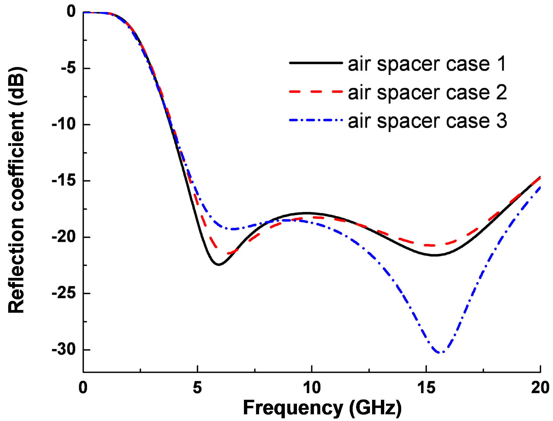
Figure 2. Reflection coefficients of the optimized results for the air-spacer type.
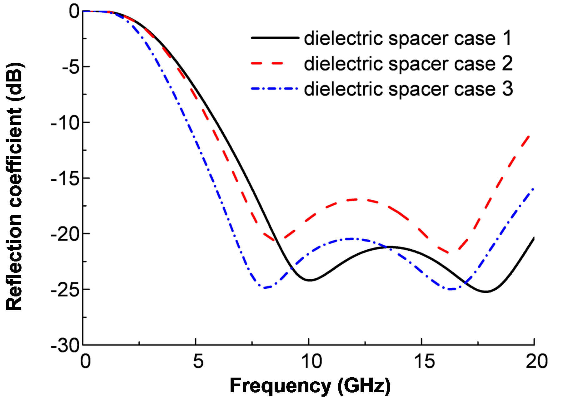
Figure 3. Reflection coefficients of the optimized results for the dielectric-spacer type.

Table 1. Parameters of air-spacer type.
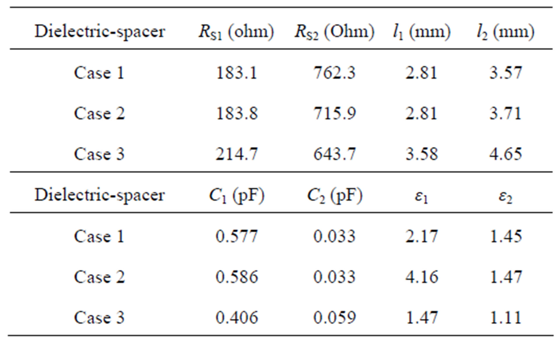
Table 2. Parameters of dielectric-spacer type.
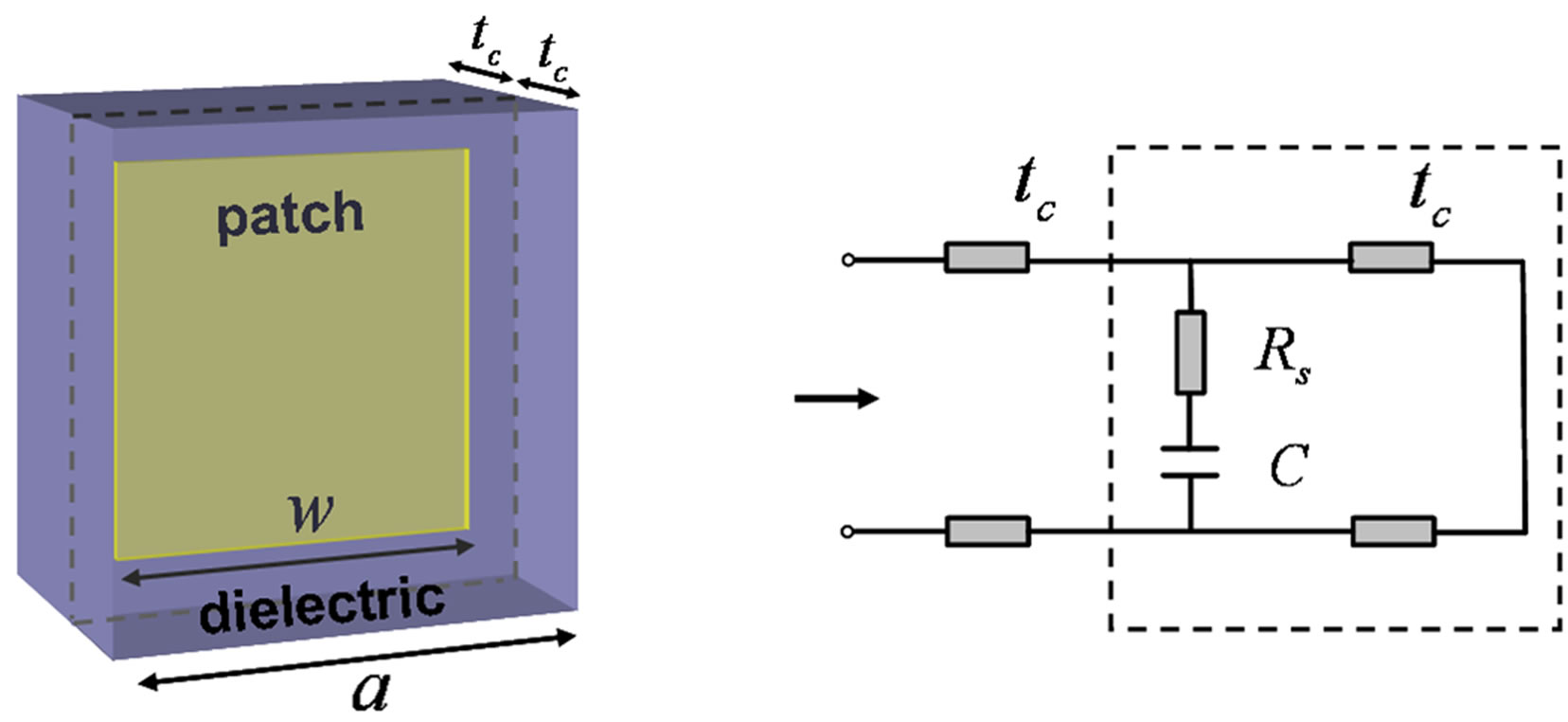
the above circuit models. Here we implement full wave simulation of the meta-surface with the help of comercial EM field simulation software—CST Microwave StudioTM. The schematic of unit cell of the meta-surface structure and its equivalent circuit model is shown in Figure 4. Figure 5 shows the comparison of the impedance Z obtained from full wave simulation and circuit model, respectively. Obviously, they coincide with each other well. Among these circuit parameters, the capacitance C in Equation (2) depends on both the dielectric layer and the patch size of the meta-surface. We need to obtain the capacitance of the patch itself and remove the influence brought by the dielectric layer.
According to transmission line circuit theory, we can obtain the equivalent admittance of the unit cell shown in Figure 4(a),
 , (7)
, (7)
where, y1 is the admittance of the half dielectric (dashed line area in Figure 4(b)) combined with the patch, η is the wave impedance of the dielectric. The equivalent admittance, y, can obtained by full wave EM simulation. From Equation (7), we can extract y1 as
 (a) (b)
Figure 4. (a) Patch embedded in dielectric medium and (b) its corresponding equivalent circuit model.
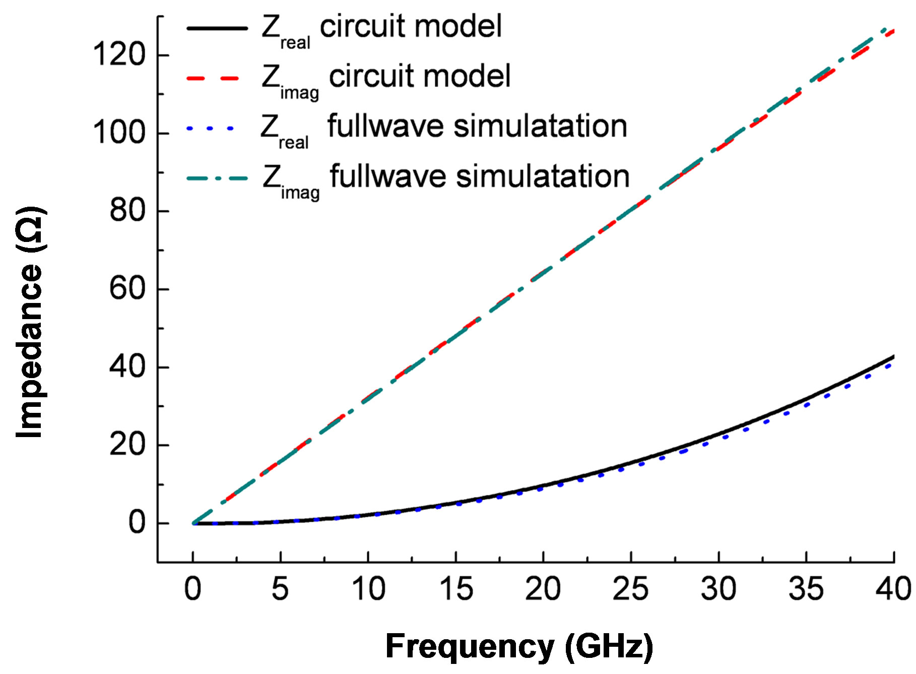
Figure 5. Impedance of the first layer obtained from the circuit model and the full wave simulation, respectively. (ε1 = 4.4, RS = 112.5 W, w/a = 6.7/6.8).
 . (8)
. (8)
Then, according to Equations (1)-(3) we can deduce the admittance b of the patch, and obtain the dispersion relation of the patch capacitance C,
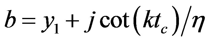 , (9)
, (9)
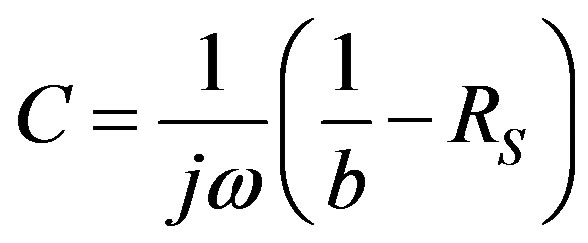 . (10)
Figure 6 shows the impact of the patch size to its related capacitance value. We can use these curves to design the patch size for realizing certain capacitance values required in Table 1 and Table 2. Using the extracted capacitance of patch meta-surface, we are able to construct the double layer absorber based on the optimized circuit model described in Table 1 and Table 2. Detailed structure and material parameters are shown in Table 3 and Table 4, corresponding to the optimal designs depicted in Figure 2 and Figure 3, respectively. Both of the two cases utilize a patch array embedded in a dielectric layer with thickness of 0.2 mm and permittivity of 4.4, respectively, to realize a large patch capacitance required in the first layer.

Figure 6. Dispersion curves of the capacitance of the patch, RS = 112.5 W, tc = 0.2 mm, a = 6.8 mm.
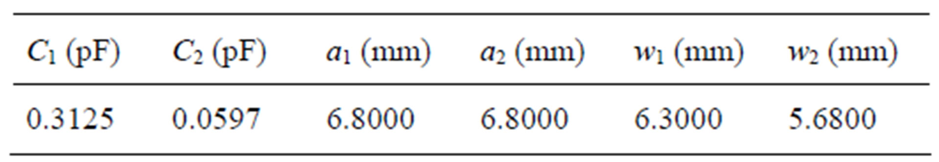
Table 3. Patch sizes to realize the capacitive value required for air-spacer case 3.
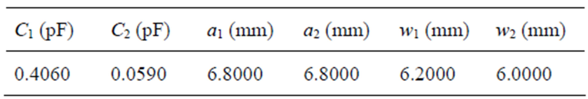
Table 4. Patch sizes to realize the capacitive value required for dielectric-spacer case 2.
5. Verification by Full Wave Simulation
Because the actual capacity of the meta-surface in the absorber structure varies with the frequency (due to the dispersion), it leads to some deviation between the results calculated from the circuit model and that from the full wave simulation. However, either Figure 7 or Figure 8" target="_self"> Figure 8 shows that the two-layer resistive meta-surface structure can achieve a stable absorption with reflection coefficient below –10 dB in a ultra-wide band (4 ~ 20 GHz).
6. Thickness Discussion
It is known that for a given frequency response, the total thickness of a magnetodielectric absorber cannot be less than a theoretical limit, which depends on the bandwidth, reflection coefficient and permittivity of the layers [9]. The constraint relation of these parameters should satisfy the following inequality,
 , (11)
where R is the reflection coefficient, l is the wavelength

Figure 7. Reflection coefficients obtained from circuit model and full wave simulation (type A).
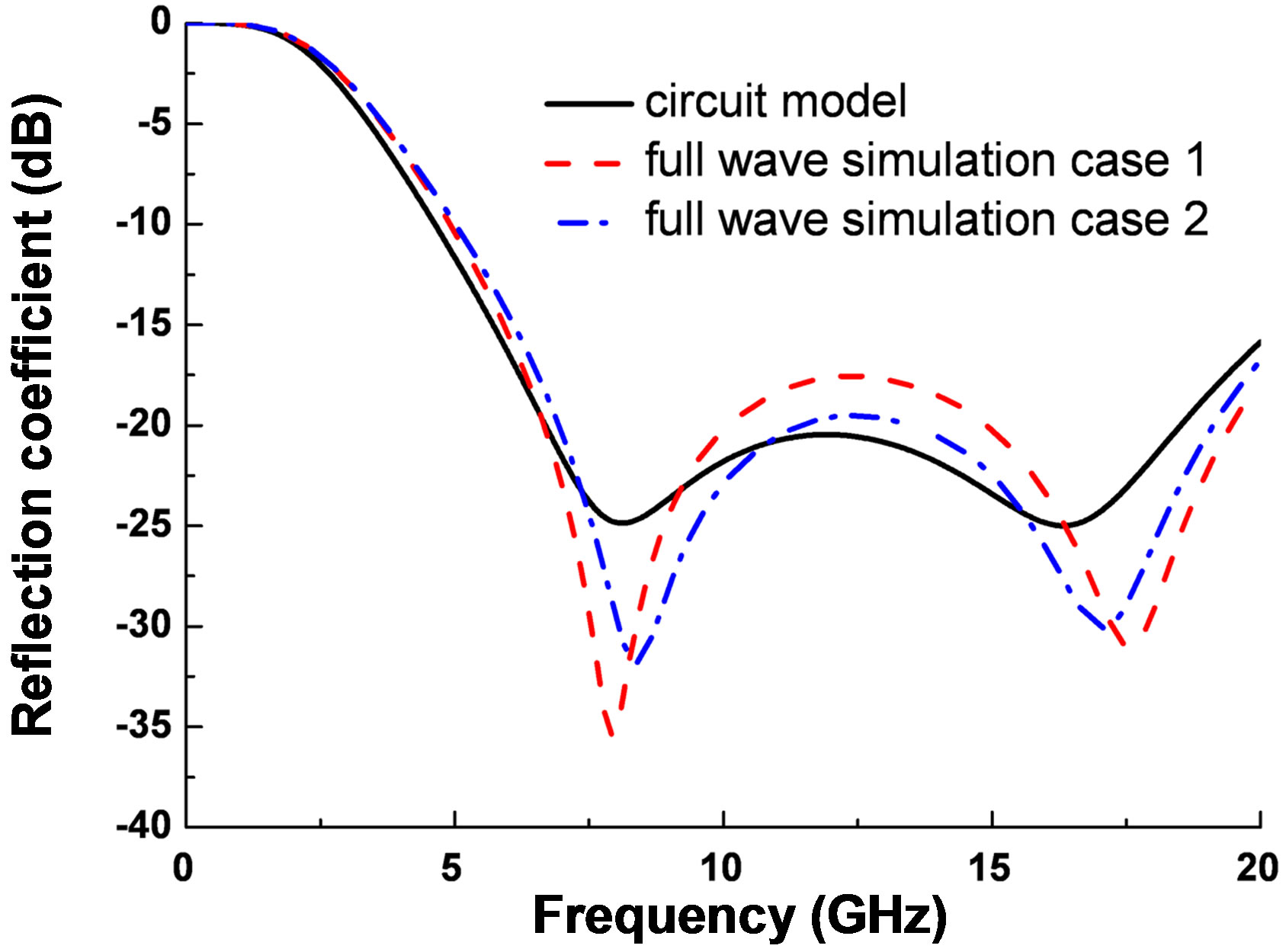
Figure 8. Reflection coefficients obtained from circuit model and full wave simulation (type B).
in free space and di, ms,i is the thickness and the static permeability of the i-th layer in the absorber. For broadband non-magnetic absorber, Equation (11) can be further approximated to
 , (12)
where R is in decibel, and the integral part is the area of the curved-top ladder between the reflection curve and the λ-axis. This relation indicates that deeper absorption requires thicker absorbers. From the reflection curve (black-solid line) in Figure 2, we can obtain the area intrgration . Substitute the integral value into Equation (12), we can obtain that the theoretical limit of the total thickness is about 9.1 mm for air-spacer type, and 8.26 mm for dielectric-spacer type, respectively. In our optimal design, the thickness of the air-spacer type is less than 9.4 mm, and that of the dielectric-spacer type is less than 8.63 mm. Both of them are quite close to that of the theoretical limit.
7. Conclusion
An optimal design of ultra-wideband (4 ~ 20 GHz) absorber composed of only two resistive meta-surface layers of patch array is reported. Gradient Descent and the GA method are successfully employed in the design to achieve minimized total thickness and ultra-wideband absorption of the structure, which make the absorber design easy to realize. By retrieving the capacitance of the meta-surface, two design examples with reasonable parameters have been given which verified the optimization procedure and the performance via full wave simulations. The proposed method could be applied in designing ultra-wideband microwave absorber for different purposes.
8. Acknowledgements
This work is supported by the National Nature Science Foundation (60990322, 60990320, 60671002, 60801001 and 6101011) and Specialized Research Fund for the Doctoral Program of Higher Education (NO. 2011009 1120052).
REFERENCES
- R. L. Fante, M. T. McCormack, T. D. Syst and M. A. Wilmington, “Reflection Properties of the Salisbury Screen,” IEEE Transaction on Antennas and Propagation, Vol. 36, No. 10, 1988, pp. 1443-1454. doi:10.1109/8.8632
- L. J. Du Toit, “The Design of Jauman Absorbers,” IEEE Antennas and Propagation Magazine, Vol. 36, No. 6, 1994, pp. 17-25. doi:10.1109/74.370526
- L. J. Du Toit and J. H. Cloete, “Electric Screen Jauman Absorber Design Algorithms,” IEEE Transaction on Microwave Theory and Technology, Vol. 44, No. 12, 1996, pp. 2238-2245. doi:10.1109/22.556452
- B. Munk, P. Munk and J. Prior, “On Designing Jaumann and Circuit Analog Absorbers (CA Absorbers) for Oblique Angle of Incidence,” IEEE Transaction on Antennas and Propagation, Vol. 55, No. 1, 2007, pp. 186-193. doi:10.1109/TAP.2006.888395
- J.-C. Liu, C.-Y. Liu, C.-P. Kuei, Y.-S. Hong and D.-C. Lou, “Periodic Hybrid FSS Screens for Broadband Microwave Absorber Design at X-Band,” Journal of Chung Cheng Institute of Technology, Vol. 34, No. 2, 2006, pp. 121-130.
- E. Yildirim and O. Aydin Civi, “Design of a Wideband Radar Absorbing Structure,” 5th European Conference on Antennas and Propagation (EUCAP), Rome, 11-15 May 2011, pp. 1403-1406.
- A. Kazemzadeh, “Nonmagnetic Ultrawideband Absorber with Optimal Thickness,” IEEE Transaction on Antennas and Propagation, Vol. 59, No. 1, 2011, pp. 135-140. doi:10.1109/TAP.2010.2090481
- B. A. Munk, “Frequency Selective Surfaces: Theory and Design,” Wiley, New York, 2000.
- K. N. Rozanov, “Ultimate Thickness to Bandwidth Ratio of Radar Absorbers,” IEEE Transaction on Antennas and Propagation, Vol. 48, No. 8, 2000, pp. 1230-1234. doi:10.1109/8.884491
NOTES
*Corresponding author.