Journal of Electromagnetic Analysis and Applications
Vol. 3 No. 11 (2011) , Article ID: 8334 , 4 pages DOI:10.4236/jemaa.2011.311069
Design and Analysis of a Novel Surface Acoustic Wave Micro Position Sensor
![]()
1Institute of Microelectronics, Chinese Academy of Sciences, Beijing, China; 2School of Information Science and Engineering, Graduate University of Chinese Academy of Sciences, Beijing, China.
Email: *kai.yang@utah.edu
Received August 9th, 2011; revised September 20th, 2011; accepted October 10th, 2011.
Keywords: SAW, Position Sensor, Reflective Grooves
ABSTRACT
In order to realize the micromation of position sensors, and extend the application area into micro scale, this paper designs a novel micro position sensor, Mace SAW (Surface Acoustic Wave) position sensor, which can be fabricated with MEMS technology. Its key components are IDTs (Interdigital Transducers) and reflective grooves. The structure and working principles of the sensor are introduced theoretically, and the manufacture process is then put forward.
1. Introduction
Position sensors are used in many industrial applications to measure the linear displacement or angular positions of objects [1]. There are many kinds of position sensors, which are on various principles, such as piezoresistive method [2], capacitive method [3-5], infrared method [6], and SAW method [7], etc.
As for micro position sensors, piezoresistive and capacitive methods are commonly used. The problem is the extremely low variation of physical quantities like resistance and capacitance on changing relative position [8]. Noise is extremely hard to determinate from sensor signal [8]. As a result, piezoresistive and capacitive micro position sensors may have far worse resolutions than macro sensors.
SAW is a non-electromagnetic wave that travels along the surface of a piezo-electric substrate [9]. SAW sensors have many merits such as high performance, small volume, ability to bear harsh working environment (e.g. hyperthermia and strong electromagnetic radiation). Compared to other technologies of position sensing, SAW method has many advantages as it doesn’t require an extra layer, and it could be implanted on surface with different materials, such as glasses or copper [10].
SAW has been used to make position sensors in macroscopic fields. For example, Matthew et al. presented an acoustic position sensing system for large scale interactive displays [11]; another typical example is the economical SAW touch panel invented by Adler et al. [7,12].
To the authors’ knowledge, micro SAW position sensor has seldom been reported.
For the sake of extending the application area into micro scale, this paper puts forwards a novel Mace SAW position sensor, which is fabricated by MEMS technology.
2. Structures and Performances
As shown in Figure 1 and Figure 2, the contour of this sensor is a square. The vertical and horizontal emitting IDTs are respectively fixed on the left upper corner and right lower corner of the glass substrate. The two corresponding receiving IDTs are fixed on the right upper corner of the glass substrate. An array of 45˚ fine reflective grooves is etched on each edge of the substrate. The piezoelectric substrate is made of Y-cut quartz, and the IDTs are made of aluminum. The wavelength of SAW is 4 times that of the width of an interdigit. The structural parameters are listed in Table 1, and the performance indexes are listed in Table 2.
3. Working Principles
3.1. Fundamental Principals
Mace SAW position sensor is based on sending, reflecting, and receiving a series of SAW across reflective grooves. When a sample (such as a bacterium) touches the sensor, the waves are absorbed, causing a touch event to be detected at that point. As shown in Figure 1, Emitter 1 and Receiver 1 are used to obtain the x-axis value of
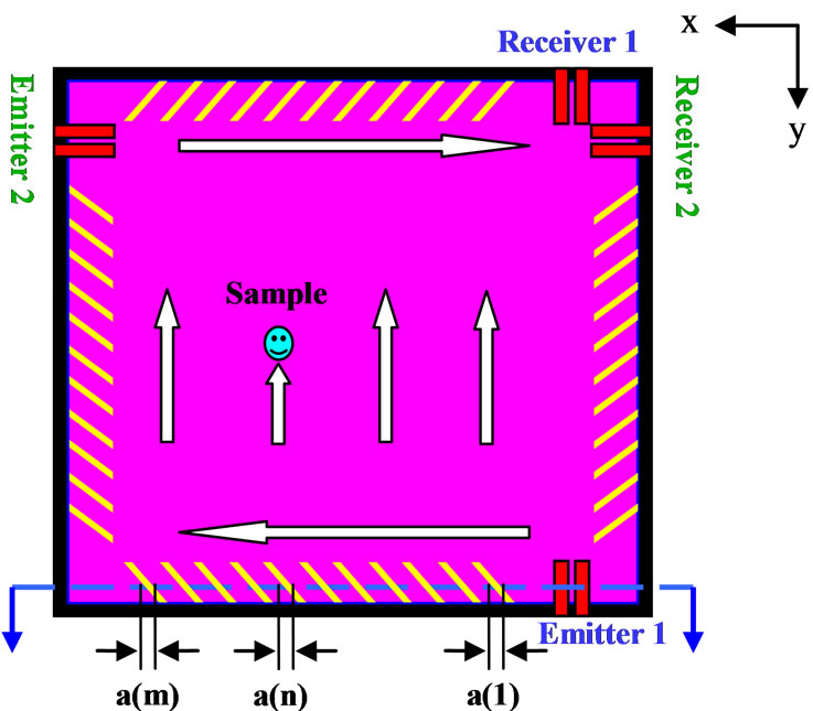
Figure 1. Top view of the sensor.
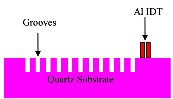
Figure 2. Sectional view of the sensor.
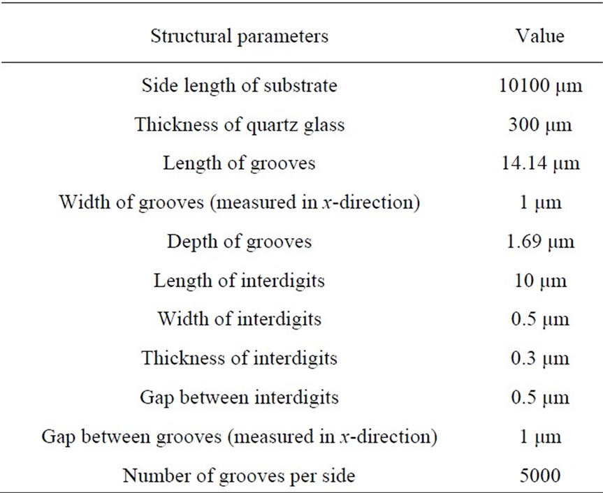
Table 1. Structural parameters of the sensor.
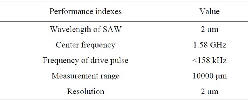
Table 2. Performance indexes of the sensor.
the sample. Emitter 1 converts the electric signals input from external circuits into SAW, which spreads left along the surface. Then, the SAW is reflected up by the array of fine reflective grooves on the lower edge and becomes an even planar transmission. Finally, the SAW is converged right into a linear transmission. Receiver 1 receives the linear transmission and converts it into electric signals for external circuits to analyze. When no sample is applied, the waveform of the received signals is an approximate squarewave. When a sample is applied, the SAW energy will be partly absorbed, and a dip will appear somewhere on the output waveform. The x-axis value of the sample can be obtained by analyzing the position of the dip. In the same way, we can also get the y-axis value of the sample using Emitter 2 and Receiver 2.
3.2. The Generation of SAW
When applying a δ-pulse voltage on the electrodes of the emitting IDTs, the δ-pulse will be converted into a halfsine wave, as shown in Figure 3.
3.3. The Addition of SAW Signals
There are 5000 reflective grooves on each edge, and the receiver will receive the addition of 5000 waves. The combination of the series of waves has an approximately square contour, as shown in Figure 4.
When a sample is placed on the film, it will result in the loss of SAW which passes it, and there will be an obvious dip on the combined waveform, as shown in Figure 5.
3.4. The Measurement of Sample Position
As Figure 5 shows, the horizontal distance between the sample and Emitter 1 is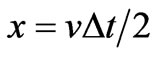 , which is obtained by measuring the delay time
  between the right margin of wave packet and the center of the dip, where v is wave velocity. In like manner, the position of the sample in Y direction can be obtained by the other pair of IDTs. It is important to mention that, the wavelength of SAW is only 2 μm, so this position sensor has a high resolution.
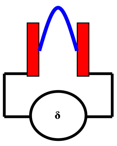
Figure 3. The generation of SAW.
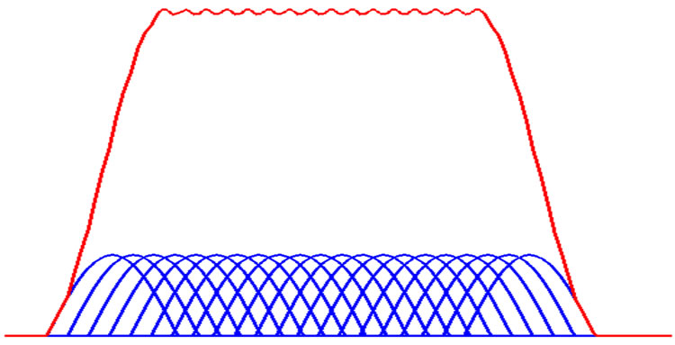
Figure 4. The combined waveform when no sample is applied.
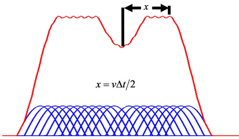
Figure 5. The combined waveform when a sample is applied.
3.5. The Design of Reflective Grooves
The amplitude reflective coefficient of SAW can be written as [13]
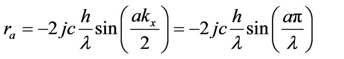 (1)
(1)
where j is , h is the depth of grooves, a is the groove width measured in x-direction (the propagation direction of the incident waves),
  is the wavelength of SAW,
  is the wavenumber of SAW, and c is a constant depending only on substrate material and orientation. For Y-cut, X-prop Quartz, c = 0.835 ± 0.025 [14].
Hence, the energy reflective coefficient of SAW can be written as
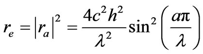 (2)
(2)
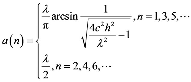
Assume that the original wave energy emitted from the emitter can be written as E(0). There are m reflective grooves on each edge, and the receiver will receive m waves finally. Proper reflective groove width a(n) (measured in x-direction, as shown in Figure 1), should be specially designed so as to ensure the amplitudes of all the m waves are equal. The wave that travels in the nth route has an experience of (n – 1) transmissions, 2 reflections, and then (n – 1) transmissions. Hence, the energy which travels in the nth route and finally reaches the receiver should be
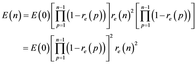 (3)
(3)
where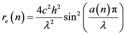 .
.
Assume that and
and  =
=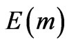 , then the expression of a(n) can be obtained by solving Equation (3)
 (4)
(4)
To assure that the expression in arcsine function locates in definitional domain, this inequality should be satisfied
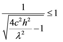 (5)
(5)
Hence
 (6)
(6)
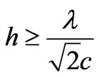
For convenience and elegance, we can set 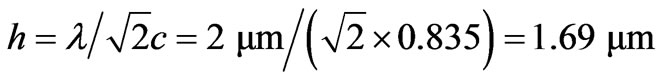 , so that
 (7)
(7)
The above formula is much more convenient and practical than the design rule in Ref. [7], because if we choose a special value for h, the reflective arrays in the sensor don’t require weighting. The design rule in this paper highly simplifies the design process.
4. Manufacture Processes
As shown in Figure 6, the manufacture process is quite concise, low cost, and possible for batch production. It only needs 3 steps: preparation of substrate, fabrication of IDTs, and fabrication of reflective grooves.
4.1. Preparation of Substrate
The Y-cut quartz needs to be rubbed, polished and cleaned with great attention in order to have low surface roughness, and make piezoelectric effect strong enough.
4.2. Fabrication of IDTs
0.3 μm thick pure aluminum film can be produced with a
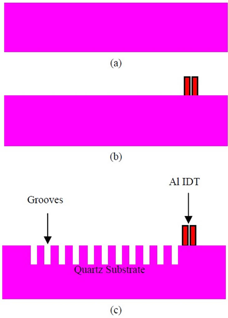
Figure 6. Manufacture process of the sensor. (a) Preparation of quartz substrate; (b) fabrication of IDTs; (c) fabrication of reflective grooves.
pure Al source in Ar gas using a sputtering system, such as Denton Discovery 18.
The width of an IDT is only 0.5 μm, so they should be patterned by electron beam exposal. Something is noteworthy in developing the pattern, because the aluminum is a kind of amphoteric metal, and the pH value of the developer should be neither too high nor too low; otherwise the margin of pattern will be etched easily.
After finishing the photolithography, Reactive Ion Etching (RIE, such as Oxford Plasmalab 80) should be applied to fabricate the IDTs. The effective factors include RF power, sort of gas, gas pressure and gas flow, etc.
4.3. Fabrication of Reflective Grooves
Similarly, the array of reflective grooves can also be patterned by electron beam exposal and etched by RIE equipment.
5. Conclusions
Mace SAW position sensor, which is presented in this paper, is a novel micro position sensor. It makes use of the merits of SAW, and is fabricated with MEMS technology. It has many advantages such as high resolution, low cost, small volume, easy to design, possible to be fabricated on quartz in batch production, etc. This sensor can be a good alternative in biology experiments, fine instruments manufacture and other related realms. It can measure position, and has the potential to measure displacement, velocity, acceleration and length. It will present high application value and great market potential.
REFERENCES
- M. Rahal and A. Demosthenous, “An Integrated Signal Conditioner for High-Frequency Inductive Position Sensors,” Measurement Science Technology, Vol. 21, No. 1, 2010, p. 015203. doi:10.1088/0957-0233/21/1/015203
- R. N. Aguilar and G. C. M. Meijer, “Fast Interface Electronics for a Resistive Touch Screen,” Proceedings of IEEE Sensors, Orlando, 12-14 June 2002, pp. 1360-1363. doi:10.1109/ICSENS.2002.1037318
- S. P. Hotelling, J. A. Strickon and B. Q. Huppi, “Multipoint touchscreen,” US Patent No. 7663607, 2010.
- S. P. Hotelling and B. R. Land, “Double-Sided TouchSensitive Panel with Shield and Drive Combined Layer,” US Patent No. 7920129, 2011.
- S. P. Hotelling, C. H. Krah and B. Q. Huppi, “Multipoint Touch Surface Controller,” US Patent No. 20090315851, 2009.
- R. W. Doering, “Infrared touch panel,” US Patent 4868912, 1989.
- R. Adler and P. J. Desmares, “An Economical Touch Panel Using SAW Absorption,” IEEE Transactions on Ultrasonics, Ferroelectrics, and Frequency Control, Vol. 34, No. 2, 1987, pp. 195-201. doi:10.1109/T-UFFC.1987.26932
- H. M. J. R. Soemers and D. M. Brouwer, “Mechatronics and micro systems,” Mechatronic Systems 2004: A Proceedings Volume from the 3rd IFAC Symposium, Sydney, 6-8 September 2004, pp. 6-8.
- R. R. Gulati, “Modern Television Practice Principles, Technology and Servicing,” 2nd Edition, New Age International Publishers, New Delhi, 2002.
- Y. Liu, J.-P. Nikolovski, M. Hafez, N. Mechbal and M. Verge, “Acoustic Wave Approach for Multi-Touch Tactile Sensing,” International Symposium on Micro-NanoMechatronics and Human Science (MHS), Nagoya, 9-11 November 2009, pp. 574-579. doi:10.1109/MHS.2009.5351748
- M. Reynolds, A. Mazalek and G. Davenport, “An Acoustic Position Sensing System for Large Scale Interactive Displays,” Proceedings of IEEE Sensors, Atlanta, 28-31 October 2007, pp. 1193-1196. doi:10.1109/ICSENS.2007.4388622
- J. Kent, M. Takeuchi and G. Laux, “Robert Adler’s Touch- screen Inventions,” IEEE International Ultrasonics Symposium, New York, 28-31 October 2007, pp. 9-20.
- D. P. Morgan, “Surface-Wave Devices for Signal Processing,” Elsevier, Amsterdam, 1985.
- J. Melngailis, R. C. Williamson, J. Holtham and R. C. M. Li, “Design of Reflective Array Surface Wave Devices,” Wave Electronics, Vol. 2, 1976, pp. 177-198.