Engineering
Vol.5 No.11A(2013), Article ID:38294,8 pages DOI:10.4236/eng.2013.511A001
A New Model for the Etching Characteristics of Corners Formed by Si{111} Planes on Si{110} Wafer Surface
MEMS and Micro/Nano Systems Laboratory, Department of Physics, Indian Institute of Technology, Hyderabad, India
Email: *prem@iith.ac.in
Copyright © 2013 Prem Pal, Sajal Sagar Singh. This is an open access article distributed under the Creative Commons Attribution License, which permits unrestricted use, distribution, and reproduction in any medium, provided the original work is properly cited.
Received June 24, 2013; revised July 24, 2013; accepted July 31, 2013
Keywords: MEMS; Silicon; Anisotropic Etching; Micromachining; KOH; TMAH; Convex Corner; Concave Corner
ABSTRACT
The etching characteristics of concave and convex corners formed in a microstructure by the intersection of {111} planes in wet anisotropic etchant are exactly opposite to each other. The convex corners are severely attacked by anisotropic etchant, while the concave corners remain unaffected. In this paper, we present a new model which explains the root cause of the initiation and advancement of undercutting phenomenon at convex corners and its absence at concave corners on {110} silicon wafers. This contrary etching characteristics of convex and concave corners is explained by utilizing the role of dangling bond in etching process and the etching behavior of the tangent plane at the convex corner. The silicon atoms at the convex edge/ridge belong to a high etch rate tangent plane as compared to {111} sidewalls, which leads to the initiation of undercutting at the convex corner. On the other hand, all the bonds of silicon atoms pertaining to concave edges/ridge are engaged with neighboring atoms and consequently contain no dangling bond, thus resulting in no-undercutting at concave edges/corners.
1. Introduction
Silicon micromachining is extensively performed using wet anisotropic etching for the fabrication of simple cavities to complex structures [1-5]. Moreover wet anisotropic etching is inevitable if the microstructures with slanted sidewalls are to be fabricated. This method of etching exploits variations in the etch rates of the low index crystallographic planes (i.e. {100}, {110}, {111}, etc.). The major advantages of wet etching include lowcost and batch process besides others, which are indispensable requirements for the minimization of fabrication cost leading to the cost reduction of the end-product. Due to these factors, silicon wet anisotropic etching is an important area of research in the field of microelectromechanical systems (MEMS).
In wet anisotropic-based bulk micromachining, the selection of wafer depends upon the type of structure to be fabricated. For instance, rectangular/square shaped cavities/grooves are fabricated in {100}Si wafers while {110}Si is used for fabricating microstructures with vertical as well as slanted sidewalls. In the {100}-oriented silicon wafer, four {111} planes, which are oriented at an angle of 54.7˚ to the wafer surface, are exposed during anisotropic etching of a circular (or arbitrary shaped) mask opening as shown in Figure 1. In the case of {110}-oriented wafer, six {111} planes are exposed as illustrated in Figure 2. These planes intersect the {110} surface in the form of a hexagon. Two of the six {111} planes emerge at <110> direction, and are oriented at an angle of 35.3˚ to the {110} wafer surface, while the other four {111} planes appear at <112> directions and are vertical to the {110} surface. The appearance of vertical planes along <112> direction makes {110} silicon wafer an appropriate choice for the formation of deep trenches/ grooves with vertical sidewalls [4-10]. In both these types of wafers, prolonged etched patterns are generally bounded by {111} planes due to their slowest etch rate nature in all kinds of anisotropic etchants.
The intersection of {111} planes form either concave corners (<180˚ i.e. corners turning inside) or convex corners (>180˚ i.e. corners turning outside), depending upon the type of structures, for instance, in the case of cavity, {111} planes form concave corners (Figure 1 and 2), while they make convex corners in the case of mesa
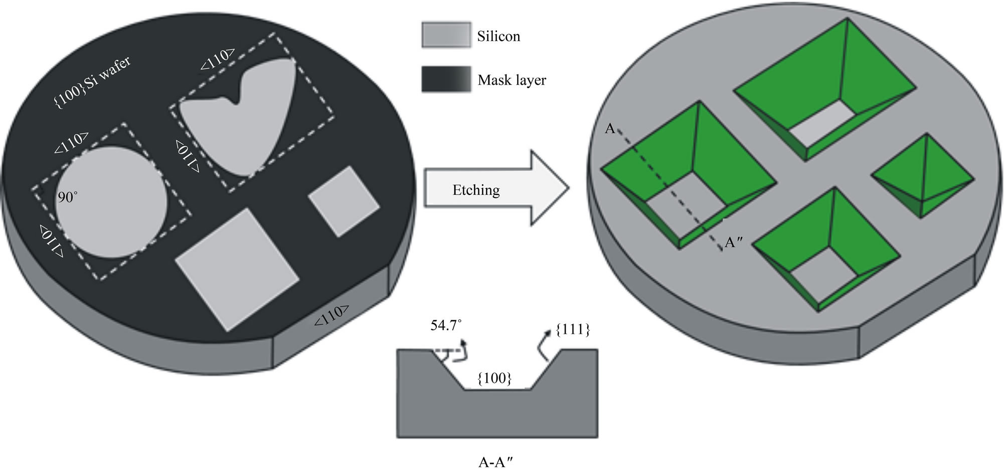
Figure 1. Wet anisotropically etched cavities with different shapes and sizes formed by {111} sidewalls in {100} Silicon wafer.
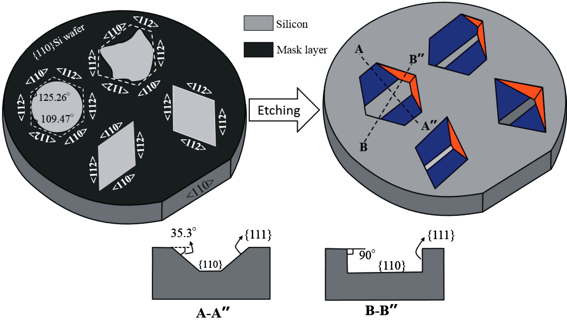
Figure 2. Wet anisotropically etched cavities with different shapes and sizes formed by {111} sidewalls in {110} Silicon wafer.
structure. Although both types of corners (i.e. convex and concave) are bounded by {111} planes, their etching characteristics are exactly opposite. The concave corner remains intact during the etching, while convex corners are immediately attacked by the etchant leading to heavy undercut. Hence the fabrication of structures with protected convex corner is a tedious task. The mechanisms of undercutting for {100}-oriented silicon wafer are widely investigated [11-16]. However, very less is reported for {110}Si wafers [17-20]. In view of the importance of {110}-oriented silicon wafer for the fabrication of microstructures with vertical sidewalls, a simple model needs to be developed to understand the initiation of undercutting at convex corners, while no-undercutting at the concave corners.
This paper presents a new model to explain the etching characteristics of concave and convex corners on {110}Si wafer. It describes the initiation of undercutting at convex corners, which are formed by the intersection of {111} planes in {110}Si wafer, during wet anisotropic etching process. Moreover it explains the inhibition of undercutting (or no-undercutting) at concave corners which are also formed by the intersection of {111} planes.
2. The Etching Characteristics of Convex and Concave Corners
There are six {111} planes that can be exposed from one side of the {110}Si wafer surface using wet anisotropic etching. These planes intersect {110} surface along <112> and <110> directions which subsequently can form a polygon with three pairs of parallel sides as shown in Figure 2. Differently oriented parallelograms and triangular geometries can be constructed using <112> and <110> directions as illustrated in Figure 3. Though the sides of a parallelogram formed by <112> directions comprises vertical sidewalls, still the slanted {111} planes are emerged at the corners R and U as presented in Figure 2. It happens mainly because the <110> directions, which comprise {111} slanted planes, are tangent to these corners.
As described in the previous section, the etching characteristics of concave and convex corners are opposite to each other. The convex corner are badly damaged in anisotropic etchants, whereas no damage occur at concave corners. As shown in Figures 2-4, {111} planes intersects each other forming either an acute angled or an obtuse angled corner. As illustrated in Figure 4, at the acute angled convex corner, the silicon atoms at the convex edge contain two dangling bonds while the {111} planes forming the edge consist of atoms with only one dangling bond. In the case of obtuse corners, the atoms of convex ridge as well as the {111} sidewalls planes comprise one dangling bond. The number of dangling bonds at the acute angled convex corner is more than the neighboring {111} planes which makes it more reactive in anisotropic etchants. As a result the acute angled convex corner experiences heavy undercutting and is badly damaged as the etching proceeds. However in the case of obtuse angled convex corner, the convex edge as well as the neighboring {111} planes consist of atoms carrying only one dangling bond, but it also encounters heavy undercut. Hence, the concept of dangling bond alone cannot be exploited to explain the undercutting at all types of corners. In this work, a very simple model is developed to explain the undercutting at all kinds of convex corners as well as the no-undercutting at concave corners.
2.1. The Model
This paper deals with different types of corners which are realized by the intersection of {111} planes only. The
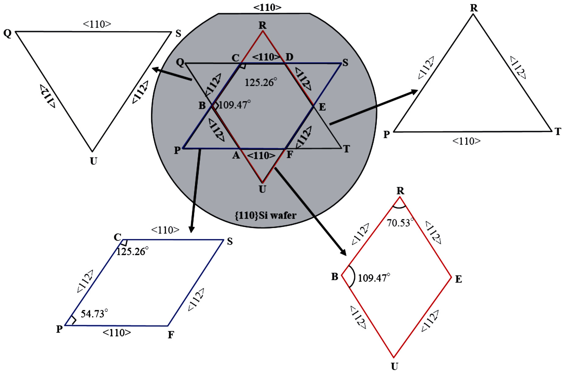
Figure 3. Schematic illustration of different shapes formed by <112> and <110> directions on {110}Si surface.
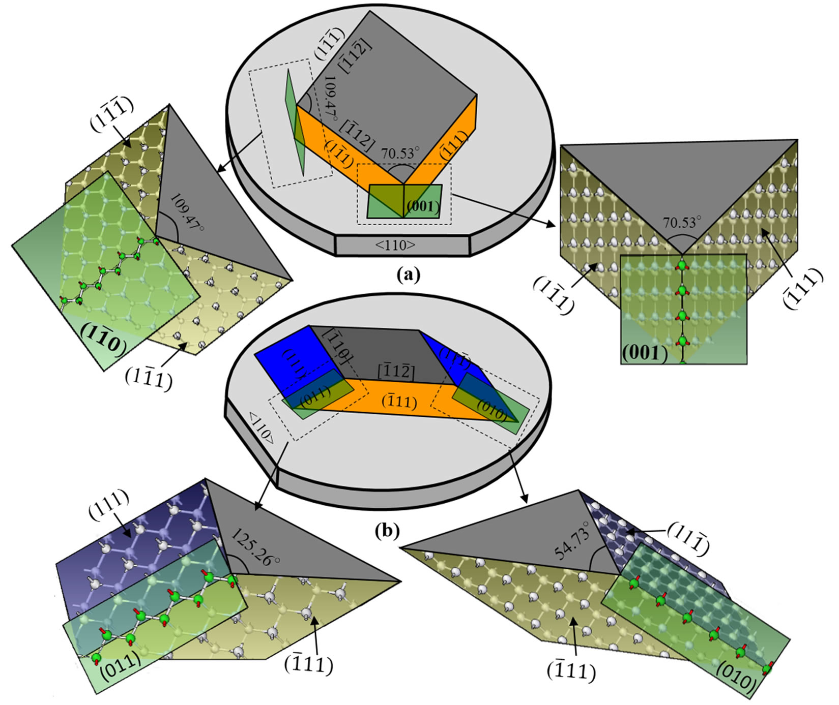
Figure 4. Schematic representation of the convex corners of the mesa structures realized on {110}Si surface by the intersection of {111} planes.
cavities formed by {111} planes comprise only concave corners (Figure 2), while the mesa structures encompasses only convex corners (Figure 4). As described above and shown schematically in Figure 4, two different arrangement of atoms are exposed at the convex corners of mesa structure: one with two dangling bonds at acute corner and the other with one dangling bond at obtuse angle. Now the question, what is the orientation of the planes to which these two arrangements of convex edged atoms belong. In order to answer this question, we can consider the planes passing through the convex edges. However there are infinite number of planes that can pass through this edge, the silicon atoms of the convex edge belongs fully to only the tangent plane at that edge as can quite simply be noticed in Figure 4. Since the number of dangling bonds of atoms at the convex ridge depends on the angle of convex corner (i.e. acute or obtuse), the orientation of tangent planes also varies from acute to obtuse corner. The tangent planes at the acute convex corners are {100}, while they are {110} on obtuse corners as shown in Figure 4. At the same time in the case of concave corners, it can be observed that the concave ridge consists of atoms with no dangling bonds i.e. all atoms of concave edge are completely engaged with neighboring atoms, as shown in Figure 5. The models presented in Figures 4 and 5 are utilized to explain the contrary etching behavior of concave and convex corners in wet anisotropic etching.
2.2. Undercutting at Convex Corners
The etching characteristics of the tangent planes at convex corners can be exploited to describe the main reason behind the undercutting at different angled convex corners (i.e. acute and obtuse). As discussed in previous section, the tangent planes at acute convex corners are {100}, while they are {110} on obtuse corners as shown in Figure 4. In all kinds of anisotropic etchants, the etch rates of {110} and {100} planes is higher than that of the {111} planes as presented in Figure 6 [21]. Therefore, the undercutting starts at convex edge as the tangent plane containing the atoms of convex ridge exhibits much higher etch rate than that of the {111} planes which form the corners. The initiation of undercutting at convex corner exposes other types of high etch rate planes. In the beginning, these planes are vicinal {110}
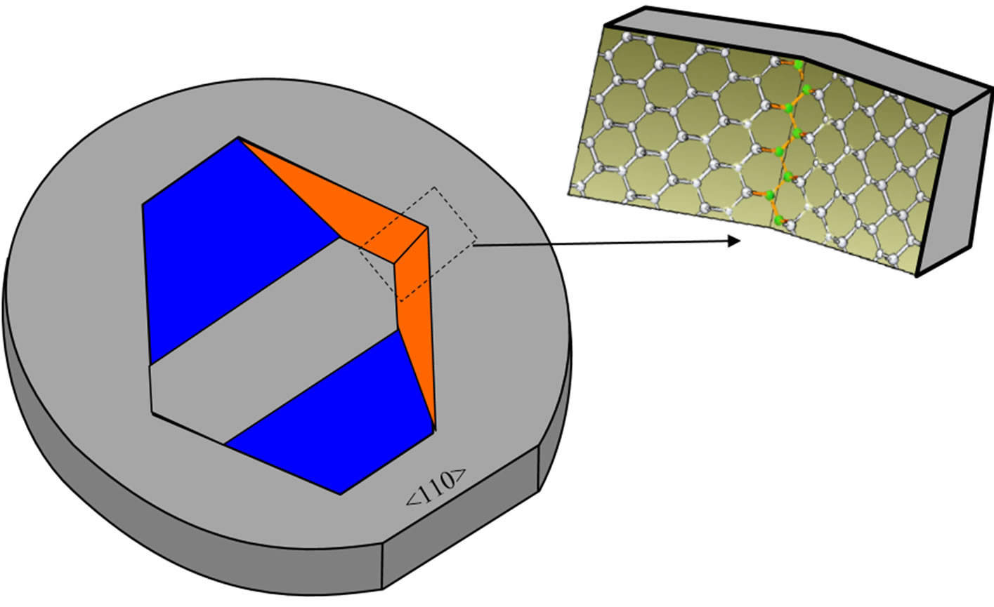
Figure 5. The arrangements of atoms at concave corners.
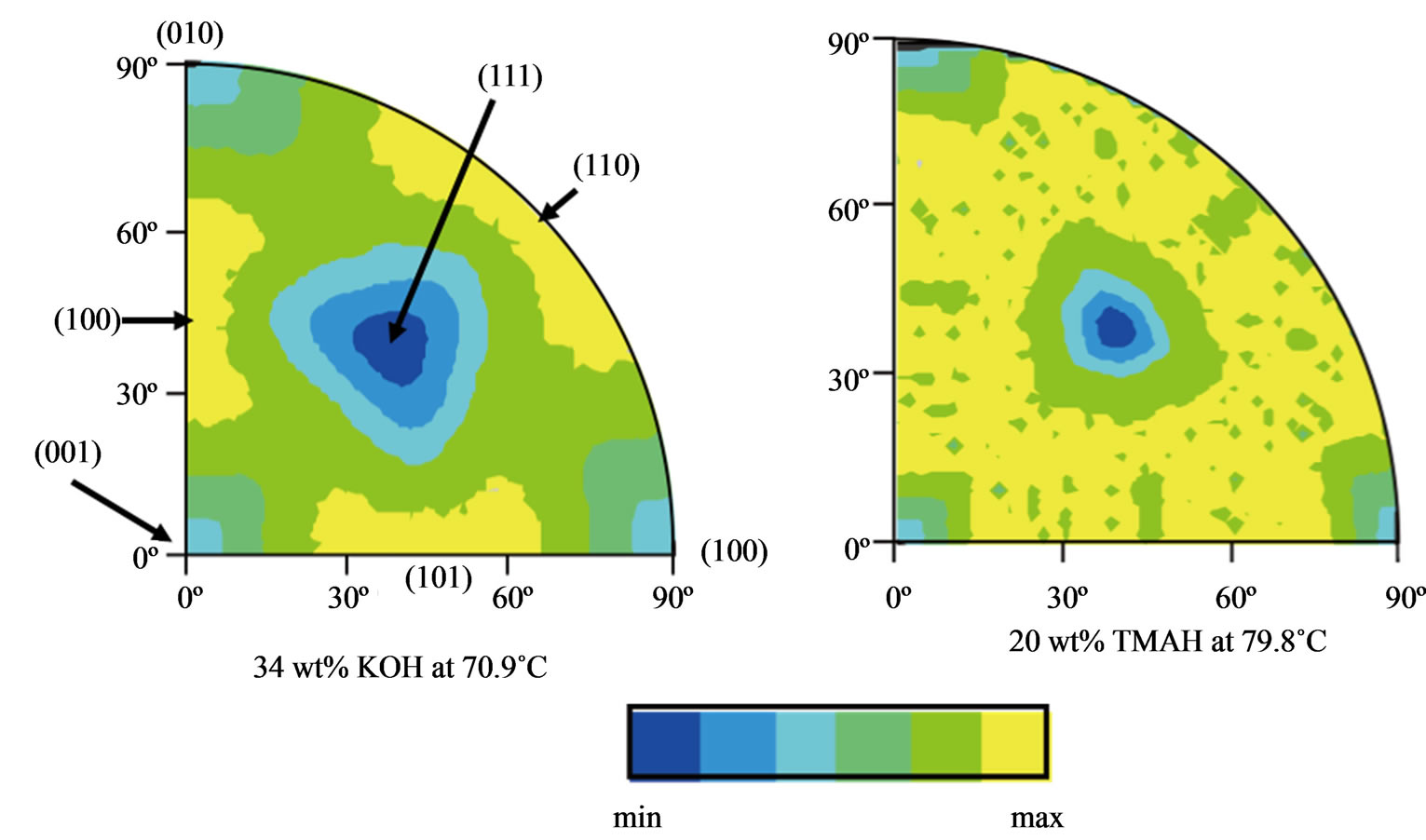
Figure 6. Comparison of the contour patterns of the etching rates in KOH and TMAH solutions [21].
(or vicinal {100}) planes, depending on the type of corner, and have high etch rates. As the process of undercutting continues, the contour of the corner is analyzed by the lateral undercutting etch rates in different directions which are estimated by the etching of a wagon wheel structure (a series of narrow and long mask opening rotated by a small angle to each other about a center) as shown in Figure 7. The lateral etch rate (or underetching) at different crystallographic directions on a plane surface depend on the type of etchant, concentration and temperature [5,22]. Hence the amount of undercutting and the geometry of the developed etch front are typically different for different etchants. The final etch front of the undercut convex corners are constructed by the intersection of directions which are parallel to the maximum lateral etch rate directions nearest to the corner. This leads to different shaped etched profile at different types of corners as can be seen in Figure 7.
The etched profile of the sidewalls appearing at the masked edges can easily be determined using WulffJaccodine method (Figure 8) [5,23,24]. In this method, the etched profile is estimated by the distribution of the etch rate vectors existing in the planes belonging to the mask edge from where the etched sidewall profile will appear. The mask edge (or line) is called the zone axis of the planes passing through it. The etch rates of the planes of any zone axis can be determined by the etch rate data of hemisphere [21,24]. The sidewall profile of the etched
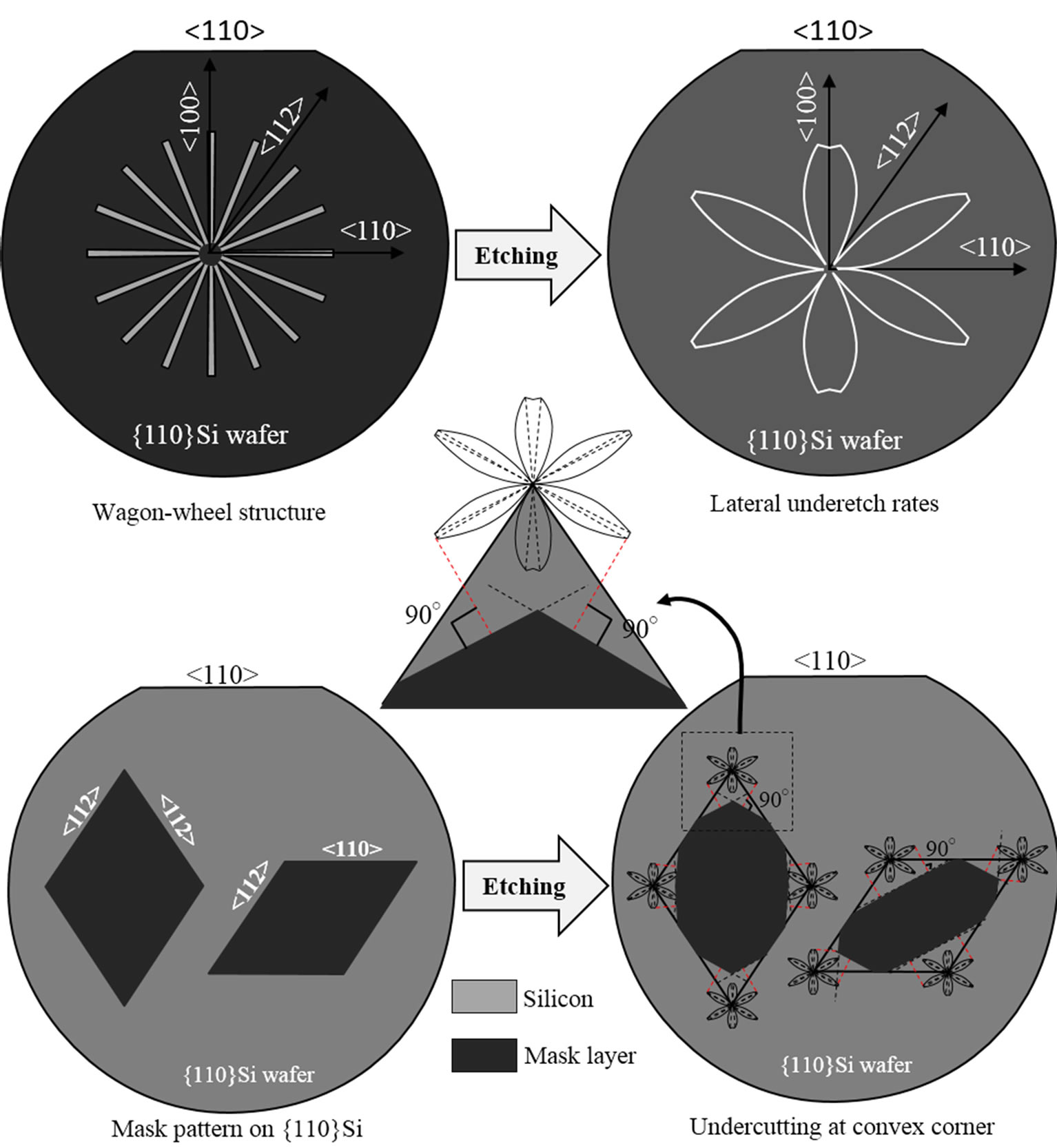
Figure 7. Lateral underetch rates as a function of orientation on silicon wafer using wagon-wheel structure (Etchant: KOH type) and its application for the determination of the etch front of convex corners.
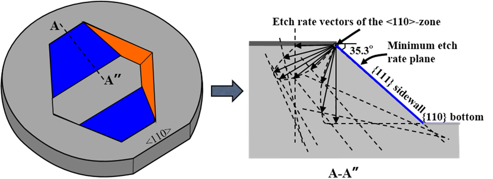
Figure 8. Schematic illustration of the estimation of sidewall profile at <110> mask edge on {110}Si surface using Wulff-Jaccodine method.
pattern at the masking edge is the minimal envelop of all intersecting lines which are perpendicular to the etch rate vectors of the different planes belonging to the mask edge (zone axis) as illustrated in Figure 8. The planes appearing at the mask edge are the minimum etch rate planes between the horizontal plane and vertical plane at that edge. Similarly the etched profile of undercut structure are estimated. In this case, the sidewalls are the minimum etch rate planes at the maximum lateral underetch rate direction.
2.3. No-Undercutting at Concave Corners
The initiation of undercutting at convex corner is explained using the etching behavior of tangent planes at those corners. The absence of undercutting at the concave corners can easily be explained by the role of dangling bonds in anisotropic etching. The increased number of dangling bond at the exposed surface enhances the removal rate of the atoms in etching solution. As presented in Figure 5, the silicon atoms pertaining to concave corner are covalently bonded with neighboring atoms. There is no unsatisfied bond left. We can state that the {111} planes, which are forming the concave corners, consist of atoms with one dangling bond, while the atoms of concave edges are engaged completely. Owing to this fact, no undercutting is initiated at the concave corners and they remain intact and firmly defined by the intersection of {111} planes regardless of the etching time, etch depth, etchant concentration and the etching temperature, as schematically shown in Figure 2.
3. Conclusion
A new model is developed to explain the undercutting at the convex corners and the no-undercutting at the concave corners, which are formed by the intersection of two {111} planes on {110} wafer surface. The present model is based on the etching characteristics of tangent planes at the convex ridge/edge and the role of dangling bonds in silicon anisotropic etching process. The tangent planes at convex ridges of acute and obtuse corners are {100} and {110} planes, respectively. The typical etch rates of these planes are much higher than that of the {111} planes whose intersection forms the convex edge. This explains the undercutting at convex corners and the noundercutting at concave corners in a very simple and effective way. The silicon atoms of concave edge do not comprise any dangling bond (i.e. all bonds are engaged) that results in inhibition of undercutting (i.e. no-undercutting) at concave corners. The proposed model is versatile and satisfactorily explains the undercutting at convex corners and the no-undercutting at concave corners in a very simple and effective way.
4. Acknowledgements
This work was supported by research grant from the Department of Science and Technology (Project No. SR/S3/ MERC/072/2011), New Delhi, India.
REFERENCES
- S. Lee, S. Park and D. Cho, “The Surface/Bulk Micromachining (SBM) Process: A New Method for Fabricating Released Microelectromechanical Systems in Single Crystal Silicon,” Journal of Microelectromechanical Systems, Vol. 8, No. 4, 1999, pp. 409-416. http://dx.doi.org/10.1109/84.809055
- B. Tang and K. Sato, “Formation of Silicon Nano Tips in Surfactant-Modified Wet Anisotropic Etching,” Applied Physics Express, Vol. 4, 2011, Article ID: 056501. http://dx.doi.org/10.1143/APEX.4.056501
- P. Pal and K. Sato, “Complex Three Dimensional Structures in Si{100} Using Wet Bulk Micromachining,” Journal of Micromechanics and Microengineering, Vol. 19, No. 10, 2009, Article ID: 105008. http://dx.doi.org/10.1088/0960-1317/19/10/105008
- I. Zubel and M. Kramkowska, “Possibilities of Extension of 3D Shapes by Bulk Micromachining of Different Si (h k l) Substrates,” Journal of Micromechanics and Microengineering, Vol. 15, No. 3, 2005, pp. 485-493. http://dx.doi.org/10.1088/0960-1317/15/3/008
- J. Frühauf, “Shape and Functional Elements of the Bulk Silicon Microtechnique: A Manual of Wet-Etched Silicon Structures,” Springer, 2005.
- J. Haneveld, H. Jansen, E. Berenschot, N. Tas and M. Elwenspoek, “Wet Anisotropic Etching for Fluidic 1D Nanochannels,” Journal of Micromechanics and Microengineering, Vol. 13, 2003, pp. S62-S66. http://dx.doi.org/10.1088/0960-1317/13/4/310
- E. S. Kalesar and M. W. Carver, “Deep Anisotropic Etching of Tapered Channels in (110)-Oriented Silicon,” Chemistry of Materials, Vol. 1, No. 6, 1989, pp. 634-639. http://dx.doi.org/10.1021/cm00006a016
- A. Lipson and E. M. Yeatman, “A 1-D Photonic Band Gap Tunable Optical Filter in (110) Silicon,” Journal of Microelectromechanical Systems, Vol. 16, No. 3, 2007, pp. 521-527. http://dx.doi.org/10.1109/JMEMS.2007.892894
- A. Holke and H. T. Henderson, “Ultra-Deep Anisotropic Etching of (110) Silicon,” Journal of Micromechanics and Microengineering, Vol. 9, No. 1, 1999, pp. 51-57. http://dx.doi.org/10.1088/0960-1317/9/1/306
- D. L. Kendall, “Vertical Etching of Silicon at Very High Aspect Ratios,” Annual Review of Materials Science, Vol. 9, 1979, pp. 373-403. http://dx.doi.org/10.1146/annurev.ms.09.080179.002105
- P. Pal, K. Sato and S. Chandra, “Fabrication Techniques of Convex Corners in a (100)-Silicon Wafer Using Bulk Micromachining: A Review,” Journal of Micromechanics and Microengineering, Vol. 17, No. 10, 2007, pp. R111- R133. http://dx.doi.org/10.1088/0960-1317/17/10/R01
- H. K. Trieu and W. Mokwa, “A Generalized Model Describing Corner Undercutting by the Experimental Analysis of TMAH/IPA,” Journal of Micromechanics and Microengineering, Vol. 8, No. 2, 1998, pp. 80-83. http://dx.doi.org/10.1088/0960-1317/8/2/009
- M. Chahoud, H. H. Wehmann and A. Schlachetzki, “Etching Simulation of Convex and Mixed InP and Si Structures,” Sensors and Actuators A, Vol. 69, 1998, pp. 251-258. http://dx.doi.org/10.1016/S0924-4247(98)00090-9
- H. Schroder and E. Obermeier, “A New Model for Si{100} Convex Corner Undercutting in Anisotropic KOH Etching,” Journal of Micromechanics and Microengineering, Vol. 10, No. 1, 2000, pp. 163-170. http://dx.doi.org/10.1088/0960-1317/10/2/311
- M. Shikida, K. Nanbara, T. Koizumi, H. Sasaki, K. Sato, M. Odagaki, M. Ando, S. Furuta and K. Asaumi, “A Model Explaining Mask-Corner Undercut Phenomena in Anisotropic Silicon Etching: A Saddle Point in the Etching-Rate Diagram,” Sensors and Actuators A, Vol. 97-98, 2000, pp. 758-763. http://dx.doi.org/10.1016/S0924-4247(02)00017-1
- W. T. Chang Chien, C. O. Chang, Y. C. Lo, Z. W. Li and C. S. Chou, “On the Miller-Indices Determination of Si{100} Convex Corner Undercut Planes,” Journal of Micromechanics and Microengineering, Vol. 15, No. 4, 2005, pp. 833-842. http://dx.doi.org/10.1088/0960-1317/15/4/022
- C. Jia, W. Dong, C. Liu, X. Zhang, J. Zhou, Z. Zhong, H. Xue, H. Zang, B. Xu and W. Chen, “Convex Corners Undercutting and Rhombus Compensation in KOH with and without IPA Solution on (110) Silicon,” Microelectronics Journal, Vol. 37, No. 11, 2006, pp. 1297-1301. http://dx.doi.org/10.1016/j.mejo.2006.07.008
- B. Kim and D. D. Cho, “Aqueous KOH Etching of Silicon (110) Etch Characteristics and Compensation Methods for Convex Corners,” Journal of The Electrochemical Society, Vol. 145, No. 7, 1998, pp. 2499-2508. http://dx.doi.org/10.1149/1.1838668
- W. Dong, X. Zhang, C. Liu, M. Li, B. Xu and W. Chen, “Mechanism for Convex Corner Undercutting of (110) Silicon in KOH,” Microelectronics Journal, Vol. 35, No. 5, 2004, pp. 417-419. http://dx.doi.org/10.1016/j.mejo.2004.01.005
- D. R. Ciarlo, “Corner Compensation Structures for (110)- Oriented Silicon,” Proceedings of the IEEE MicroRobots and Teleoperators Workshop, Hyannis, 1987.
- M. Shikida, K. Sato, K. Tokoro and D. Uchikawa, “Differences in Anisotropic Etching Properties of KOH and TMAH Solutions,” Sensors and Actuators A, Vol. 80, No. 2, 2000, pp. 179-188. http://dx.doi.org/10.1016/S0924-4247(99)00264-2
- H. Seidel, L. Csepregi, A. Heuberger and H. Baumgartel, “Anisotropic Etching of Crystaline Silicon in Alkaline Solutions,” Journal of the Electrochemical Society, Vol. 137, No. 11, 1990, pp. 3613-3631.
- R. J. Jaccodine, “Use of Modified Free Energy Theorems to Predict Equilibrium Growing and Etching Shapes,” Journal of Applied Physics, Vol. 33, No. 8, 1962, pp. 2643-2647. http://dx.doi.org/10.1063/1.1729036
- P. Pal, M. A. Gosalvez and K. Sato, “Silicon Micromachining Based on Surfactant-Added Tetramethyl Ammonium Hydroxide: Etching Mechanism and Advanced Application,” Japanese Journal of Applied Physics, Vol. 49, 2010, Article ID: 056702. http://dx.doi.org/10.1143/JJAP.49.056702
NOTES
*Corresponding author.