Materials Sciences and Applications
Vol. 4 No. 5A (2013) , Article ID: 31479 , 7 pages DOI:10.4236/msa.2013.45A001
Electrically-Conductive Composite Nanomaterial with Multi-Walled Carbon Nanotubes
![]()
1National Research University of Electronic Technology (MIET), Moscow, Russia; 2Institute of Nanotechnology of Microelectronics, RAS, Moscow, Russia; 3Scientific Manufacturing Complex “Technological Centre”, Moscow, Russia.
Email: *leo852@Inbox.ru
Copyright © 2013 Levan Ichkitidze et al. This is an open access article distributed under the Creative Commons Attribution License, which permits unrestricted use, distribution, and reproduction in any medium, provided the original work is properly cited.
Received February 6th, 2013; revised March 22nd, 2013; accepted April 11th, 2013
Keywords: multiwalled carbon nanotubes; electroconductive nanomaterial; Substrates; Carboxymethyl Cellulose; Electroconductive Gel; Electroconductive Layers
ABSTRACT
Specific conductivity ![]() of the composite nanomaterial layers with micron and submicron dimensions, consisting of carboxymethyl cellulose (CMC) and multiwalled carbon nanotubes (MWCNT) was investigated. Ultradispersed aqueous suspension was deposited on soft (aluminum foil, plates made from polyester and polyimide, cotton fabric, office paper) and solid (coverslip, silicon wafers with silicon oxide layer) substrates by silk-screen printing. Electrical resistance was measured by four-probe method and by the method of square on surface from which the conductivity
of the composite nanomaterial layers with micron and submicron dimensions, consisting of carboxymethyl cellulose (CMC) and multiwalled carbon nanotubes (MWCNT) was investigated. Ultradispersed aqueous suspension was deposited on soft (aluminum foil, plates made from polyester and polyimide, cotton fabric, office paper) and solid (coverslip, silicon wafers with silicon oxide layer) substrates by silk-screen printing. Electrical resistance was measured by four-probe method and by the method of square on surface from which the conductivity ![]() and conductivity per square of surface were calculated taking into account layer’s geometric dimensions. Specific conductivity of the layers with thickness range 0.5 - 5 µm was
and conductivity per square of surface were calculated taking into account layer’s geometric dimensions. Specific conductivity of the layers with thickness range 0.5 - 5 µm was , and max conductivity per square was ~ 0.2 S. Investigated nanomaterial is attractive to electronic and biomedical applications.
1. Introduction
Carbon nanotubes (CNT) (single-walled (SWCNT) and multi-walled CNT (MWCNT)) possess a number of unique properties (mechanical, thermal, electrical) and the special interest is their high specific conductivity![]() . On the basis of accumulated results we can conclude that CNT have a great perspective in nanoelectronics because the use of CNT nanowires is more advantageous as compared with the wires made from other materials. In fact, carbon nanotubes, layers, films, wires based on CNT have higher mechanical parameters as compared with metal nanoconductors (especially the values of breaking strength and modulus of elasticity). When one creates micro and nanoelectronical devices based on flexible substrates (flexible electronics) the most important are acceptable mechanical and conducting properties of the film materials based on CNT than based on well-known semiconductor and metal materials. It should be noted that for CNT the ratios of the breaking strength derivative (~10 GPa [1]) and specific conductivity (
. On the basis of accumulated results we can conclude that CNT have a great perspective in nanoelectronics because the use of CNT nanowires is more advantageous as compared with the wires made from other materials. In fact, carbon nanotubes, layers, films, wires based on CNT have higher mechanical parameters as compared with metal nanoconductors (especially the values of breaking strength and modulus of elasticity). When one creates micro and nanoelectronical devices based on flexible substrates (flexible electronics) the most important are acceptable mechanical and conducting properties of the film materials based on CNT than based on well-known semiconductor and metal materials. It should be noted that for CNT the ratios of the breaking strength derivative (~10 GPa [1]) and specific conductivity (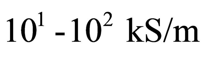
![]() [2]) to the material density is several orders of magnitude greater than ones for Cu or Al films and wires that are commonly used in microelectronics [3,4]. For example in Cu nanowires the value of the current density
[2]) to the material density is several orders of magnitude greater than ones for Cu or Al films and wires that are commonly used in microelectronics [3,4]. For example in Cu nanowires the value of the current density  was achieved several orders of magnitude smaller than in CNT wires -
 at which the material starts to fail. Developed prototypes of cable based on MWCNT doped by iodine possess high current carry capability about ~
 at room temperature [5]. Such capability is comparable with the constructional current carry capability of the cable based on superconductive materials with operating temperature of liquid nitrogen [6].
In the layers that consist of randomly interlaced SWCNT (in the form of entangled macaroni, so-called buckypaper) it was observed the high conductivity σ ~ 10 - 50  [7], and in the layers where SWCNT were in one direction it was obtained the record conductivity
 ![]()
 [8]. We note that experimentally obtained specific conductivity of the layers is worse than calculated values
  for individual SWCNT. The layers of buckypaper based on MWCNT also possess the high
 ![]() about ~10 kS/m, and their electrical properties are highly dependent on many factors including the kind of MWCNT and the purification [9,10]. By now experimental layers of buckypaper with MWCNT are much inferior to the calculated values of the individual specific conductivity
about ~10 kS/m, and their electrical properties are highly dependent on many factors including the kind of MWCNT and the purification [9,10]. By now experimental layers of buckypaper with MWCNT are much inferior to the calculated values of the individual specific conductivity  for MWCNT [11,12].
High values of the conductivity and aspect ratio of CNT allow us to create on their basis composite conductive materials with extremely low percentage of CNT filler to reach the percolation threshold. Particularly, in the polymer matrix made from polyurethane with MWCNT filler the percolation threshold was obtained at the concentration C = 0.13 wt% [13], and in the matrix made from carboxymethyl cellulose (CMC) the percolation threshold was obtained at the concentration C = 0.1 - 0.25 wt% MWCNT [14].
In general MWCNT are safer for environmental conditions and for public health [15] than SWCNT or soot, and are more inexpensive than SWCNT. MWCNT provide good mechanical and conducting properties, low percolation threshold in composite materials, they are the subject of the extensive research, purpose of which is creating nanomaterials based on them with various unique properties.
In this article we present the preliminary results of investigated conductivity of the layers made from nanomaterials deposited on various substrates and containing composition from: matrix—CMC, filler—MWCNT. Layers were deposited on various substrates: soft— polyimide (PI), polyester (PE), aluminum foil (AF), cotton fabric (CF) and office paper “Ballet −80 gr/m2” (OP); solid: Si wafers with silicon oxide film (Si/SiΟ2) and coverslips (CS).
2. Samples Preparation and Measurement Techniques
Bimetallic catalyst Fe-Мo/МgO was used in MWCNT fabrication. MWCNT synthesis was performed at t ~ 900˚C in the flow of Ar and CH4 for 40 min. Achieved material was oxidized in 8.8 М hydrogen peroxide solution for 1 hour for stable aqueous suspension. MWCNT mass concentration in finished material was 95 ± 1 wt%. In this case the following intermediate procedures were performed: purification, drying etc, which are described in detail in [16].
In our experiments we used electrically-conductive gel (ECG) in the form of carboxymethyl cellulose aqueous solution ((~4 wt% CMC), specific conductivity of which was  at t = 25˚C in the electric field with intensity ~ 100 V/m. ECG served as a matrix for the fabrication of conductive nanomaterial. It was thoroughly mixed mechanically in a magnetic stirrer and ultrasonic (US) bath for about 1 hour and about 0.5 hours, respectively. MWCNT filler was added in finished matrix, after that the aqueous dispersion consisting of ECG and MWCNT was subjected to mix in a magnetic stirrer and US bath for ~1.5 hours and ~1.5 hours, respectively.
There were also prepared control samples based on ECG without MWCNT and samples based on ECG and soot K-354. In the last case soot particles had micron and submicron dimensions. In all dispersions concentration ratio of carbon particles were the same ~5 wt%. Thus, in sample preparation were used: ECG solution—4 wt% CMC (#1), dispersion with 4 wt% CMC + 5 wt% MWCNT (#2), dispersion with 4 wt% CMC + 5 wt% soot К-354 (#3). Assigned numbers fit with the numbers of layer’s series that were achieved from relevant solutions or dispersion. Sample #1 and #3 were the control samples, sample #2 was the object of study.
Layers were deposited on all kinds of substrate at same conditions by silk-screen printing, i.e. layers were deposited on the substrate through the stencil in the form of square with dimensions 20 × 20 mm2 or in the form of rectangle with dimensions 20 × 30 mm2. All series of dispersions possess very good adhesion on CF and OP substrate, and the worst adhesion was on Si/SiΟ2 and CS substrates. Thereby, surfaces of these substrates were subjected to extra washing and ion-chemical treatment in vacuum. Layers on the substrates were dried at ≈30˚C for 60 hours. Final samples were measured; the measurements were repeated after annealing in the air at 180˚C for 30 min or after annealing in the hydrogen environment at 200˚C for 30 min.
All electrical measurements were performed in “current source” mode. The current was in the range i = 100 nA - 10 ma, mounted current value  varied in the range ±0.1%. Measuring probes and appearance of the samples are shown in Figure 1.
Before each measurement probe contacts were carefully cleaned which reduced inaccuracy of measurements and gave good agreement between results obtained under repeated measurements. In the case of four-probe measurements the probes were placed linearly with constant
 (a) (b)
Figure 1. Measuring probes for: (a) two-probe method (resistance per square of the surface), sample on CS substrate; (b) four-probe method (1, sample on OP substrate; 2, sidewall probe with silver tip; 3, the screw for probe pressing force control).
distance  mm from each other. The probes had silver contacts. Measuring probes was pressed to sample surface by special control screw (see Figure 1(b), 3) which allowed controlling the pressing force of the probes to the sample1.
Sample conductivity was measured by both two-probe method (see Figure 1) and four-probe method (see Figure 2(a)). In first case conductivity per square  of surface was measured. In second one, specific bulk conductivity
![]() . In both cases from measured current value, voltage and layer thickness the specific bulk conductivity
. In both cases from measured current value, voltage and layer thickness the specific bulk conductivity ![]() was measured by the formula
was measured by the formula
 (1)
(1)
The value  defined as
 , where
 ![]() was calculated from the Formula (1). Specific conductivities estimated from the measured values of the parameters according to (1) and from
was calculated from the Formula (1). Specific conductivities estimated from the measured values of the parameters according to (1) and from  values differed by less than 15% - 20%, which indicated a good uniformity of investigated layers and respected conditions for twoprobe and four-probe measurements in our experiments. In both cases, the measurements were made in two different points of the sample, which located mutually
 (a)
(a)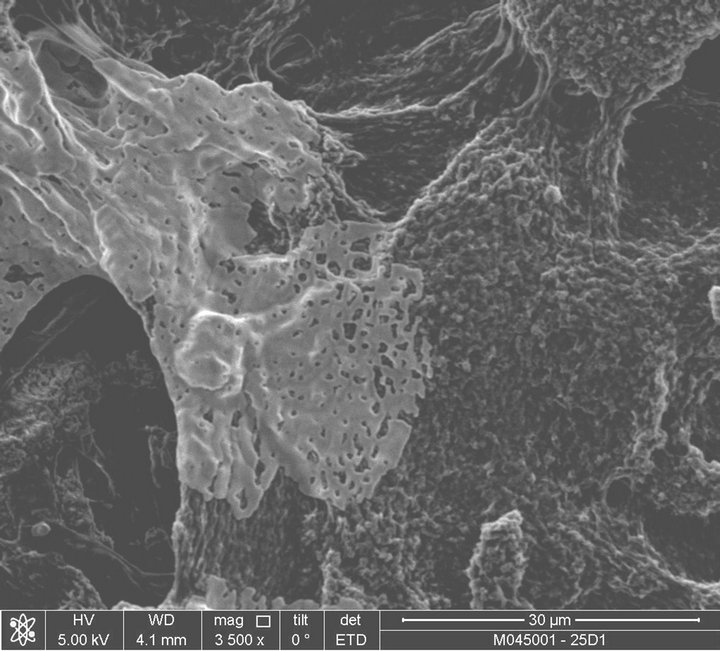 (b)
(b)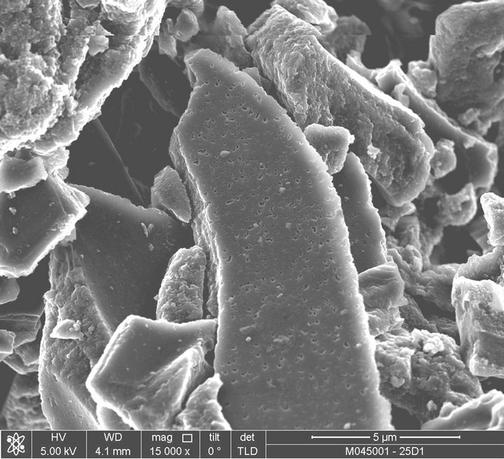 (c)
(c)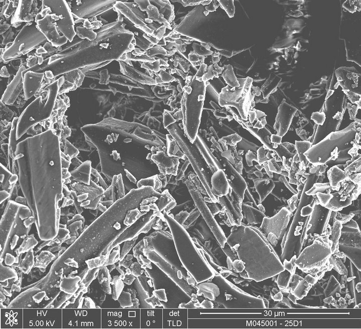 (d)
(d)
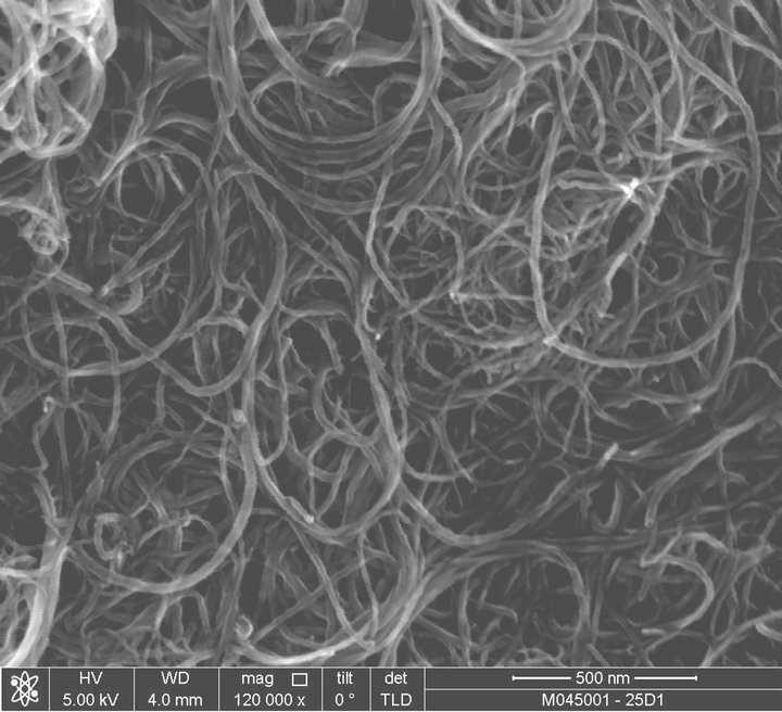
Figure 2. Typical SEM images of the layers from series #2 (a,b) and #3 (c,d) on SiΟ2 substrates. Layers thickness ≈5 µm: layer from the series #2, (a) scale 30 µm, (b) scale 500 nm; layer from series #3, (c) scale 30 µm, (d) 500 nm.
transverse to each other, and the average values ![]() and
and  were defined.
The thickness ![]() of the layers on substrates was estimated by interference technique and micrometer technique. In both cases the relative accuracy of
of the layers on substrates was estimated by interference technique and micrometer technique. In both cases the relative accuracy of ![]() value didn’t exceed 15% - 20% from the average value. The value
value didn’t exceed 15% - 20% from the average value. The value ![]() for investigated layers was fixed in the range ~0.5 - 80 µm.
for investigated layers was fixed in the range ~0.5 - 80 µm.
3. Experimental Results and Discussion
Images of the layers deposited on CS and Si/SiΟ2 substrates were done by scanning electron microscopy (SEM). As a part of study we obtained the images of ECG matrix and fillers from MWCNT, ECG and K-354 soot. Typical SEM images of the layers from series #2 (a,b) and #3 (c,d) on Si/SiΟ2 substrates are shown in Figure 2. There are an appreciable difference between images: MWCNT filler consist of long (³3 µm) filamentous tubes with diameter £30 nm (Figures 2(a) and (b)), and soot filler consist of granular conglomerates with wide range of linear dimensions (1 - 20 µm) (Figures 2(c) and (d)).
The electrical measurements for ECG solution showed that at t » 20˚C the conductivity was σ ~ 0.5 S/m, and temperature coefficient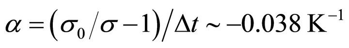 , where
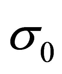 —specific conductivity at
 ,
, —temperature range in region ∆t ≈ 0 - 70˚C. However, mentioned parameters of the samples from series #1 significantly reduced after annealing in air and hydrogen environments (
 S/m,
S/m, ). Therefore we could suppose that drying and annealing significantly reduce the concentration of the charge carriers.
Annealing of the samples with MWCNT (series #2) in air and hydrogen environments led to significantly increase in conductivity. In the case with air annealing the ![]() values increased several times (<5); in the case with hydrogen annealing the
values increased several times (<5); in the case with hydrogen annealing the ![]() values increased up to 200 times as compared with conductivity of the samples before the annealing. Higher
values increased up to 200 times as compared with conductivity of the samples before the annealing. Higher ![]() values were achieved in the layers with low thickness (<5 µm) because in thick layers numerous cracks and pores were formed which disturb the wholeness of the samples. Measured and calculated data from certain samples with achieved maximum s values are shown in Table 1.
values were achieved in the layers with low thickness (<5 µm) because in thick layers numerous cracks and pores were formed which disturb the wholeness of the samples. Measured and calculated data from certain samples with achieved maximum s values are shown in Table 1.
As seen from Table 1, in the samples that were done without annealing by deposition on soft substrate (OP, PE, CF) the layers with MWCNT (series #2) had 2 - 5 times higher values of specific conductivity as compared with the samples on solid substrates (CS, Si/SiΟ2). However, the situation dramatically changes after annealing: ![]() value is several times higher in the layers on solid substrate than on soft OP and CF substrates.
value is several times higher in the layers on solid substrate than on soft OP and CF substrates.
Maximum values of conductivity per square of surface were in the range . In control layers, that didn’t consist the MWCNT (see Table 1, series #1) or contained the particles of soot K-354 (see Table 1, series #3), values of
 ![]() were 5 - 7 orders of magnitude smaller than for the layers based on MWCNT (see Table 1, series #2).
were 5 - 7 orders of magnitude smaller than for the layers based on MWCNT (see Table 1, series #2).
Such high specific conductivity in investigated layers from series #2 relative to the other series #1 and #3 apparently due to the following factors: higher aspect ratio for MWCNT 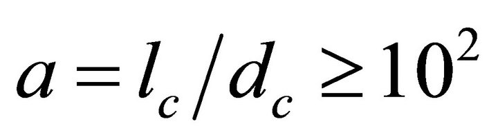 (lc—CNT height,
 — CNT diameter); their high value of individual specific conductivity
 ; optimal composition of nanomaterial, that consist of poorly conducting matrix (CMC) and highly conducting filler (MWCNT). Such nanomaterial composition during annealing provides an efficient removal of polymer organics, which results in highly conductive nanotube and conductive graphitic residue that fill space between tubes and thus increase the conductivity of the layer.
Samples based on MWCNT (series #2 and #3) are composite materials, and the analytical calculation of the effective conductivity  is a great challenge. With
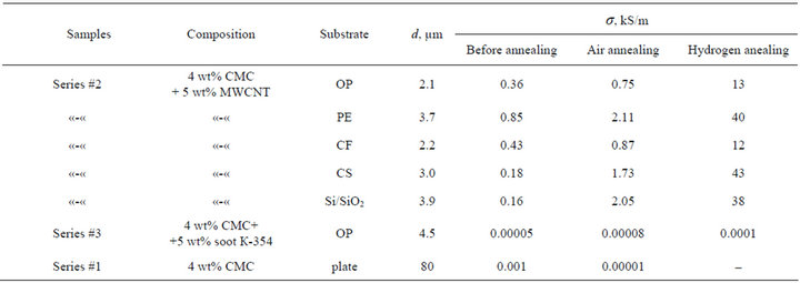
Table 1. Certain characteristics of typical samples with maximum values of typical samples with maximum values of s.
some approximation it could be possible to estimate the value , when matrix is homogeneous and one kind of filler is uniformly distributed in the volume [17]:
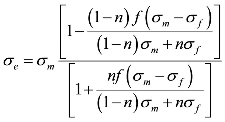 , (2)
, (2)
where —specific conductivity of the matrix,
 — specific conductivity of the filler, i.e. the ratio of the inclusion volume to the volume of the sample,
![]() —form factor of the inclusion particles along one of the principal axis, which is concur with depolarization factor and in the case of CNT is equal to
—form factor of the inclusion particles along one of the principal axis, which is concur with depolarization factor and in the case of CNT is equal to . According to (1) it is followed that the value of
  significantly depends on the parameters
  and
and![]() , for example with a strong filling
, for example with a strong filling  we have
 , (3)
, (3)
According to (1) and (2) the effective conductivity of the composite material increases rapidly with decreasing ![]() and with increasing
and with increasing . In our experiment:
 , where was taken into account
  for MWCNT that we used (see p.1); filling factor2
  , due to fact that MWCNT serves as a filler.
We performed the comparison between calculated  from (1) and (2) and measured
 ![]() (from Table 1) data. They strongly differ—measured
(from Table 1) data. They strongly differ—measured ![]() were several orders of magnitude greater than calculated
were several orders of magnitude greater than calculated . In the fact, classic expressions (1) and (2) allow us to define effective specific conductivity of the composite material when filler particles are oriented and isolated from each other by parts of the matrix. In this case the change of
  greater depends on the variation of the parameters
 ,
, ![]() and
and  than on
 , for example with f » 0.05,
  and
and  the value
  have the order of £10-1 S/m, and with
  and the same other parameters –σe~10 S/m. Even minimum measured value σ » 360 S/m for composite nanomaterial 4 wt% CMC + 5wt% MWCNT (see Table 1) is much higher than the highest estimated value of the σe ~10 S/m that was calculated by Formula (2).
Large difference (by more than 3 - 4 orders of magnitude) between measured and estimated specific conductivities suggests the fact that MWCNT particles are located in the matrix in intertangled not isolated states with the formation of electrical contacts between them. By all appearances, random and numerous electrical contacts between MWCNT create conductive infinite and parallel clusters, which are the reason of high specific conductivity in the investigated layers. It can be assumed that the contacts between MWCNT particles are tunnel and their transparence (i.e. their conductivity) determines the conductivity of the infinite cluster. From these assumptions, it follows that effective specific conductivity of composite nanomaterial will depends on the density of infinite conductive clusters and on their specific conductivity.
Apparently, the proposed mechanism of conductivity is implemented in the investigated layers of composite nanomaterials based on MWCNTs. In above mentioned experiment the annealing increases the number of tunnel contacts and their contact conductivity, increases the number of parallel-connected clusters and their overall specific conductivity.
Let us estimate  for extreme case, when all MWCNTs are involved in the formation of conductive infinite clusters that have fully transparent electric contacts between themselves which are located in the matrix with negligible specific conductivity. In this case the layers with dimensions 20 mm × 20 mm × 3 μm could be described as equivalent to the layers from densely packed MWCNTs with approximate dimensions 7 mm × 7 mm × 1 μm. Here we take into account that the filler parameter of the MWCNTs in our experiments is
 , and that 1/3 part from overall MWCNTs could be involved in conductivity on preferential direction. Then, for equivalent layer from MWCNT we estimate
 , where
  and
and , which is lot more than measured values
 .
.
According to this, we could assume that there is a potential for increasing values ![]() and
and  in the investigated layers at the expense of increasing the transparency of tunnel contacts between MWCNTs in the matrix of nanomaterial. Apparently, we had reached such positive effect when
 ![]() and
and  were enhanced for 3 - 4 order after the annealing of the samples in air and hydrogen environments.
Degradation research didn’t show significant changes in s value at numerous bends of soft substrate. After numerous bends of the layers (180˚ bend, bending radius 1 mm, the cycle-300 times) the conductivity changed no more than ±20% relative to baseline values. After numerous bends the layers didn’t peel off from substrate, didn’t crack and saved their prior appearance.
4. Conclusions
The layers of the composite nanomaterial which was done from aqueous dispersion consisted of 4 wt% CMC and 5 wt% MWCNT on soft and solid substrates were fabricated and investigated. Conductivities of the layers significantly increased after the annealing of the samples in air environment (up to 5 times) or hydrogen environment (up to 200 times). The samples of the composite nanomaterial based on MWCNT possessed by 4 - 6 orders of magnitude higher conductivity values than the control samples based on CMC, or CMC and soot K-354. Obtained values of specific bulk conductivity (~40 kS/m) and surface conductivity (~0.2 S) had the same orders which were obtained for the layers of buckypaper based on both MWCNT [7] and SWCNT [18]. Numerous bends of soft substrates didn’t affect on conductivity of the layers with thickness £5 µm.
Measured conductivity of the samples was several orders of magnitude higher than calculated conductivities for classic composite materials. We assumed that conductive infinite clusters from MWCNT were formed in the investigated composite nanomaterials. Based on this assumption we had established the steps for increase the conductivity of the composite material via the increase in the transparency of the tunnel junctions that formed in the contact points of MWCNT.
Thus, investigated composite nanomaterial possesses high specific conductivity and good adhesion on the soft flexible substrates, and also it represents a perspective material for different applications (flexible electronics, conductive glues, protection of electronic circuits, devices, and biological objects from electromagnetic radiation, the growing of conductive biological tissues (nerve cells, muscles etc.); conductive paints, working in resistive heating mode on aircrafts surface for the prevention of forming or heating of the ice etc.) [19].
5. Acknowledgements
This work was partly funded by Russian Ministry of Education (Government contract №16.426.11.0043 from 12.09.2011), and by The Russian Foundation for Basic Research (project No.12-08-12014/12 from 15.11.2012).
REFERENCES
- N. Grobert, “Carbon Nanotubes: Becoming Clean,” Materials Today, Vol. 10, No. 1-2, 2007, pp. 28-35. doi:10.1016/S1369-7021(06)71789-8
- Z. W. Pan, S. S. Xie, B. Chang, et al., “Very Long Carbon Nanotubes,” Nature, Vol. 394, 1998, pp. 631-632. doi:10.1038/29206
- Q. Ngo, A. M. Cassell, A. J. Austin, et al., “Characteristics of Aligned Carbon Nanofibers for Interconnect via Applications,” IEEE Electron Device Letters, No. 4, 2006, pp. 221-224. doi:10.1109/LED.2006.870865
- D. Fabris, T. Saito, T. Yamada, X. Sun, P. Wilhite and C. Y. Yang, “Current Capacity and Thermal Transport in Carbon Nanofiber Interconnects,” 4th IEEE International Conference on Nano/Micro Engineered and Molecular Systems, 2009, pp. 848-853. http://doi.ieeecomputersociety.org/10.1109/NEMS.2009.5068708
- Y. Zhao, J. Wei, R. Vajtai, P. M. Ajayan and E. Barrera, “Iodine Doped Carbon Nanotube Cables Exceeding Specific Electrical Conductivity of Metals,” Scientific Re ports, Vol. 1, 2011, p. 83. doi:10.1038/srep00083
- S. Mukoyama, M. Yagi, H. Hirata, M. Suzuki, S. Nagaya, N. Kashima and Y. Shiohara, “Development of YBCO High-c Superconducting Power Cables,” Furukawa Review, No. 35, 2009, pp. 18-22.
- D. Wang, D. Song, C. Liu, W. Wu and S. Fan, “Highly Oriented Carbon Nanotube Papers Made of Aligned Carbon Nanotubes,” Nanotechnology, Vol. 19, No. 7, 2008, Article ID: 075609. doi:10.1088/0957-4484/19/7/075609
- J. M. Hone, C. Llaguno, N. M. Nemes, A. T. Johnson, E. J. Fischer, D. A. Walters, M. J. Casavant, J. Schmidt and R. E. Smalley, “Electrical and Thermal Transport Properties of Magnetically Aligned Single Wall Carbon Nanotube Films,” Applied Physics Letters, Vol. 77, No. 5, 2000, pp. 666-668. doi:10.1063/1.127079
- M.-Y. Tsai, C.-Y. Yu, C.-H. Yang, N.-H. Tai, T.-P. Perng, C.-M. Tu, Z. H. Khan, Y.-C. Liao and C.-C. Chi, “Electrical Transport Properties of Individual Disordered Multiwalled Carbon Nanotubes,” Applied Physics Letters, Vol. 89, No. 19, 2006, Article ID: 192115. doi:10.1063/1.2387875
- K. Yang, J. He, P. Puneet, Z. Su, M. J. Skove, J. Gaillard, T. M. Tritt and A. M. Rao, “Tuning Electrical and Thermal Connectivity in Multiwalled Carbon Nanotube Buckypaper,” Journal of Physics: Condensed Matter, Vol. 22, No. 33, 2010, Article ID: 334215. doi:10.1088/0953-8984/22/33/334215
- H. J. Li, W. G. Lu, J. J. Li, X. D. Bai and C. Z. Gu “Measurements of the Current through a Single Multiwalled Carbon Nanotube Demonstrate a High Conduction Capacity, Which Would Be Important if Such Tubes Were Used in Integrated Circuits,” Applied Physics Letters, Vol. 95, No. 8, 2005, Article ID: 086601. doi:10.1103/PhysRevLett.95.086601
- P. Kim, L. Shi, A. Majumdar and P. L. McEuen, “Thermal Transport Measurements of Individual Multiwalled Nanotubes,” Physical Review Letters, Vol. 87, No. 21, 2001, Article ID: 215502. doi:10.1103/PhysRevLett.87.215502
- R. Zhang, A. Dowden, M. Baxendale and T. Peijs, “Conductive Network Formation in the Melt of Carbon Nanotube Thermoplastic Polyurethane Composite,” Composite Science and Technology, Vol. 69, No. 10, 2009, pp. 1499- 1504. doi:10.1016/j.compscitech.2008.11.039
- L. P. Ichkitidze and V. M. Podgaetsky, O. V. Ponomareva, and S. V. Selishchev, “Mechanical Properties of Bulk Nanocomposite Obtained by Laser Irradiation”, Izvestiya VUZov. Physica (Russia), Vol. 53, No. 2-3, 2010, pp. 125-129.
- L. P. Ichkitidze and I. V. Komlev, “Carbon Nanotubes and Composite Nanomaterials: Toxicity,” In: Lasers in Science, Engineering, Medicine. Sat. Scientific Papers, edited by VA Petrov, a society named AS Popov AS Popov (Russia), No. 21, 2010, pp. 103-113.
- L. P. Ichkitidze, T. S. Ryndina, S. V. Selishchev, O. V. Ponomareva, L. V. Tabulina, B. G. Shulizky, V. A. Galperin, Y. P. Shaman and E. V. Blagov, “Bulk Composite Nanomaterial Based on Protein and Multiwall Carbon Nanotubes,” Nano and Microsystems Technique (Russia), No. 3, 2012, pp. 13-19.
- Y. V. Kornushin, “About Effective Conductivity of Composite Materials,” Laters in Journal of Technical Physics (Russia), Vol.36, No. 9, 2010, pp. 50-53.
- A. S. Lobach, L. I. Buravov, N. G. Spitzina, A. V. Elezky, A. P. Dementev and K. I. Maslakov, “The Study of Electrical Resistivity of the Films of Single-Walled Carbon Nanotubes at Temperature Ranges 4.2-290 К,” High Energy Chemistry (Russia), Vol. 45, No. 4, 2011, pp. 360- 366.
- A. M. Heintz, An-C. Christiaen, R. B. Vijayendran, D. J. Elhard, R. S. Lalgudi, W. B. Robbins, A. b. Gupta and J. Cafmeye, “Electrical Conductive Coating Composition,” US Patent 2010/0126981 A1, 2010.
NOTES
*Corresponding author.

1In determining of the value  relative accuracy was <1 % because following conditons were respected: The ratio of distance
  (from the edges of the sample to the first probe) to value
  exceeds 2, and the layer thickness
  was much smaller than
 .
.
2Filling factor approximately the same as specific part of MWCNT (concentration 5%) due to the fact that there is a small difference in the density of the matrix (ECG—1.4 g/cm3) and in the density of the filler (MWCNT – 1.6 g/cm3) and we assume .
.