Circuits and Systems
Vol.05 No.08(2014), Article ID:48609,10 pages
10.4236/cs.2014.58020
CMOS Phase and Quadrature Pulsed Differential Oscillators Coupled through Microstrip Delay-Lines
Francesco Stilgenbauer, Stefano Perticaroli, Fabrizio Palma
Department of Information Engineering, Electronics and Telecommunications, “Sapienza - University of Rome”, Rome, Italy
Email: francesco.stilgenbauer@gmail.com, perticaroli@die.uniroma1.it, palma@die.uniroma1.it
Copyright © 2014 by authors and Scientific Research Publishing Inc.
This work is licensed under the Creative Commons Attribution International License (CC BY).
http://creativecommons.org/licenses/by/4.0/


Received 29 May 2014; revised 3 July 2014; accepted 11 July 2014
ABSTRACT
An innovative solution to design phase and quadrature pulsed coupled oscillators systems through electromagnetic waveguides is described in this paper. Each oscillator is constituted by an LC differential resonator refilled through a couple of current pulse generator circuits. The phase and quadrature coupling between the two differential oscillators is achieved using delayed replicas of generated fundamentals from a resonator as driving signal of pulse generator injecting in the other resonator. The delayed replicas are obtained by microstrip-based delay-lines. A 2.4 - 2.5 GHz VCO has been implemented in a 150 nm RF CMOS process. Simulations showed at 1 MHz offset a phase noise of −139.9 dBc/Hz and a FOM of −189.1 dB.
Keywords:
Voltage Controlled Oscillator, Microstrip, Delay-Line, Phase and Quadrature, Phase Noise

1. Introduction
Pushed from the ever-increasing demand in the electronic devices market for personal mobile devices and for wireless sensor networks, the research on innovative techniques for lowering energy requirements and costs of the electronic hardware is an extensively treated subject. At the core of every of above mentioned device, certainly an RF-IC resides, since it accomplish the necessary functional block for the establishment of a RF communication. In particular, the upconversion/downconversion task in RF-ICs usually represents the subsystems involving the major wafer area and power consumption. Toward the reduction of both areas occupation and power are placed CMOS Pulsed Bias Oscillators (PBOs). The PBO approach represents a technique exploiting the time-varying properties of electronic oscillators system. This technique can be applied to oscillators constituted of harmonic resonators refilled by active devices acting as current generators. This oscillator class aims to reach high performance in terms of phase noise with reduced energy requirements with respect to their non-pulsed counterparts. Basing on the results of Floquet Theory applied to a single oscillator [1] , we extended the pulsed bias concept to a coupled phase and quadrature system in [2] . We proved that the pulsed bias approach allows to minimize noise injection onto the Floquet Eigenvector with unitary eigenvalue, leading to decrease phase noise of generated fundamental in particular at low frequency offsets [3] [4] . However, in the effective implementation of pulsed bias architectures, the introduction of a delay is necessary for proper positioning of refilling current pulses. In the most common way, a delay can be obtained with the charging of a capacitor through a dissipative media [5] . Unfortunately, using an RC-based delay is not possible to set the pulse width independently from the pulse position. This issue is explained considering that, in the cascading of lumped elements circuits, the total delay time strictly depends on the number of stages and how they are connected. In this paper we propose a circuital solution based on the joint use of decoupling stages from resonator and of microstrip delay-lines capable to break such constraint and, at the same time, to establish coupling among oscillators with a desired phase relation. The paper is organized as follows. In Section 2 the proposed architecture is introduced, focusing on the explanation of the concept for the coupling between two oscillators in phase and quadrature. In Section 3 the theoretical analysis of the delay-line is pursued and insights for proper design are derived. In Section 4 the implementation on RF CMOS process is reported and simulation comparison with a non-pulsed architecture built in the same technology is discussed as well as a comparison with literature is given.
2. Proposed Architecture
The outputs of a phase and quadrature oscillator are phase shifted replicas of a fundamental frequency  as drawn in Figure 1.
The voltage maximum of a delayed sinusoid from a resonator can be hence used to generate refilling pulses, synchronized at output voltage minimum of another resonator. Thus in this paper, we propose to couple two oscillators applying a fixed delay of  where
where . In particular we choose to realize the delay by a microstrip transmission-line.
In a lossless transmission-line the secondary constants , characteristic line impedance, and
 , propagation constant, are both real number. The voltage of the transmission-line equation as a function of the
  is given by
 . If the load is matched to the
 , the contribution of the regressive term
  is neg-
ligible and the transfer function between the input port, at , and the output port,
  , of the transmission-line results in
 (1)
(1)
where  is the total line length.
If  has linear increase with frequency, the transmission-line behaves as a delay-line. The delay
  is related to the
 , through
 (2)
(2)
where  is evaluated at the fundamental frequency
  along with
 . Hence, the value of
  is es-
tablished considering the condition  holds. For the refilling of all the tanks, four transmission-lines
in a phase and quadrature PBO (PQPBO) are needed.
The reference schematic of the oscillator is presented in Figure 2. The system is formed by four coupled LC tanks, subdivided in two blocks,  and
and , respectively. The two inductances of every single block are implemented by center tapped inductors. All the capacitances are implemented by MIM capacitors. The value of
  and
and  were set to obtain operative center frequency of
 , suitable for ISM applications, according to
 .
.
The losses are compensated by the introduction of the current pulse generators (PG) as showed in Figure 2. The PG circuit is reported in Figure 3.
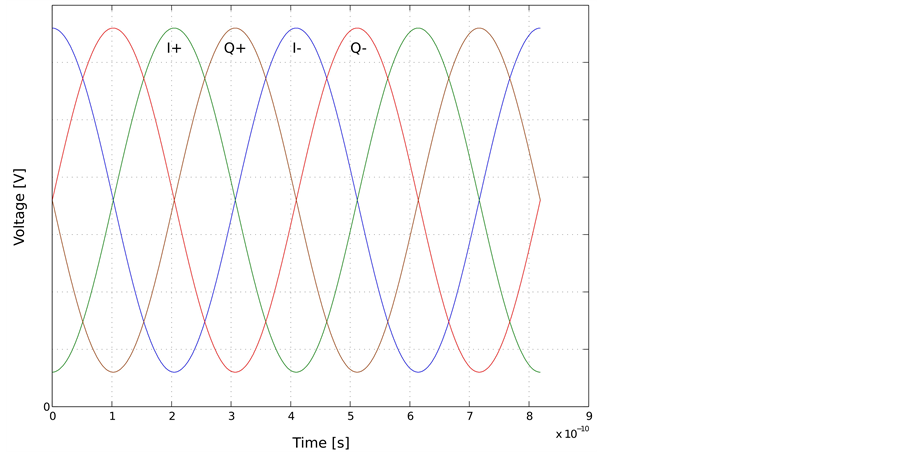
Figure 1. Typical output signals of a phase and quadrature oscillator.
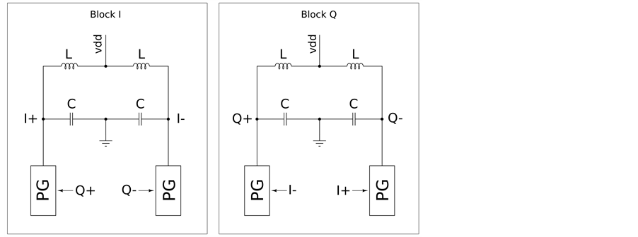
Figure 2. Oscillator schematic of the proposed PQPBO.
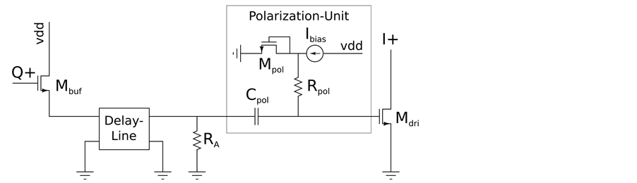
Figure 3. Pulse generator schematic.
The following description refers to the PG recharging the  tank node and driven by the signal coming from
  tank node. The buffer transistor
  provides to decouple the Delay-Line (DL) from the source tank
 , in order to prevent energy absorption by the PG. The observed impedance at the DL input is
  once the DL load is matched. Then the decoupling stage is implemented as a source-follower with a resistive load as reported in Figure 3. In order to maximize the voltage transfer between the gate and the source of
 , both the input capacitance
  and the body effect must be taken into account. A practical rule for initial sizing of
  is to set its length to the process minimum and to determine the upper bound for its width using
 (3)
(3)
This bound grants an effective isolation of the resonator from the loading effect of PG input. Then, a triple- well is used to connect the  bulk at its source voltage rather than to global ground. To avoid a large power consumption in the decoupling stage a sub-optimum value for the
  transconductance must be chosen. The
 transconductance, modeled in quadratic region, results in
 , where
 ,
,
 are carriers mobility and oxide capacitance per unit area of the adopted technology and
 ,
,  are
are
transistor width and length, respectively. If  is inferred from geometrical consideration (ne-
glecting the dependence on transistor operating region), we can derive an upper bound for . In fact, de-
scending from Equation (3) it implies  and, thus, the transconductance bound results in
 (4)
(4)
This bound must be accounted because an eventual low  reduces the source dynamics. It worth to notice that, since the source-follower is active only if the
  threshold is reached, in a C-class pulse generating system driven by the large oscillating signal this represents an advantage. In fact, the decoupling stage takes part in the pulse shaping even though the desired pulse width and positioning cannot be set in this stage.
To this aim, the DL is introduced to obtain the delay necessary to synchronize the refilling instant. The values of  and
and  are determined through literature formulas [6] [7] for a microstrip structure, whereas the dimensions of the strip width
 , height
  and the interposed dielectric relative electric permittivity
  are consistent with the process specifications. Values of the transmission-line secondary constants represent here only a first order of approximation of the integrated waveguide, since both the dissipation effects and the presence of a dielectric over the strip are ignored. Such constants result in
  and
and , where
  is the speed of light in vacuum once a quasi-TEM mode of propagation in the strip has been assumed. Referring again to Figure 3, the matching resistance
  in introduced to add one more degree of freedom in minimization of the reverse wave contribution in the DL. The DL matching technique is discussed after the description of PG stages.
The Polarization-Unit (PU), formed by ,
,  ,
,  and
and , achieves the task to fix the DC value of
the driver transistor gate  in order to set its operative region in C-class region. Further, the PU grants the proper start-up of the oscillator, since the gate node voltage of
  is initially at
  and then settles to the required n-MOS sub-threshold value. The
  has obviously the role of decoupling DC voltage of
  gate and of blocking DC current flow to reverse DL path, however for its proper sizing both input capacitance
  of driver transistor and the time constant
 , involved in the operating point voltage settling, must be accounted. Again, a practical rule for
  sizing suggests to take
 (5)
(5)
and, descending from this choice, the derivation of the equivalent resistance,  , and capacitance,
  , for calculating
 , results in
 (6)
(6)
where  is the
  transconductance and
  represents the impedance of the quar-
ter-wave DL transformer loaded by the source follower. In  calculation the parallel branch resistance of
 transistor has been neglected, since the gate node capacitance
  relates to a time constant with a more
rapid exponential decay than , which does not alter the final settling voltage. If the desired time for the oscillator stabilization is identified in
 , hence the condition for dimensioning
  is derived from
  (exponential decay approaches the final value within
  error).
 (7)
(7)
We notice in  expression only the couple
 ,
,  can be effectively adjusted to set the proper
 .
.
Finally, the  transistor generates a current pulse that re-inject charge in the destination tank
 . The sizing of the driver transistor of the PG is chosen to fulfill at least two times the Barkhausen criterion, once the resonator losses,
  , related to resonator RLC parallel model, have been determined. The criterion is expressed in
 (8)
(8)
It worth noticing the  parameter is calculated assuming the highest overdrive voltage with the gate voltage at
  as the
  transistors were arranged in a standard crossed pair architecture. This assumption leads to potentially over-estimate the necessary driver transconductance when it is operating in C-class region. In fact it is expected that C-class operation, representing a more efficient energy refilling, may allow to decrease the effective
  size in actual design of oscillator.
Follows the DL matching description. In first approximation, DL is described with its secondary constants  and
and  in lossless case. The reflection coefficient at the load of the line is
 . The load
  of the DL is formed by
  and the input capacitance
  of the
  transistor, since the PU at
  is negligible because
  and
and  behave as a short and an open circuit, respectively. Being reflection coefficient expressed as
 where
where , the condition
  cannot be
imposed because of the resistive matching, but the value of  can be minimized with a proper value of
 . The values range of
  is obtained through the testing of the input capacitance of several sizing for
 .
.
In Figure 4 the reflection coefficient as a function of  is reported for
  and
and . The minimum of
  is given by setting
  and this optimum has been achieved through fine dimensioning of
  in simulations.
The delay-line is characterized by the transfer function on the  variable
 (9)
(9)
that takes into account . The value of
  obtained with Equation (2) must be hence reduced to satisfy the
condition  in Equation (9) at fundamental frequency, which is the dominant spectral component in the signal into the PG.
3. Delay-Line implementation
The DL unit is implemented through a waveguide structure such a microstrip. As a first microstrip design step, literature formulas [6] [7] can be used to obtain the desired  and
and . Further, foundry process constraints have to be accounted especially in the microstrip sizing. To this aim, CST Microwave Studio™ was used to obtain a proper sizing of the microstrip. In order to reach a trade-off between the value of
  and minimization of resistive losses, an intermediate metallization level in chip back-end has been chosen. Below the microstrip there are an interposed dielectric and a patterned ground-plane in a lower metallization level. At sides and above, the microstrip is surrounded by a dielectric, followed by a final passivation layer on top of the die. The microstrip width
  is about
  and the interposed dielectric thickness
  is
is . In order to obtain a feasible waveguide structure in a given area, the microstrip distribution has been folded into meanders.
In Figure 5 a detail of the microstrip layout is reported. In black the basic module of the meander is highlighted in red. In detail of layout  is the distance between two neighbouring strips,
  is the length of a meander and
  is total length of the structure. In order to reduce the radiation loss of the waveguide we adopt smoothing of the corners as reported in Figure 5. Unfortunately, the optimum solution proposed in [8] is unrealizable since, in our case, it leads to width zone of the corners lower than that allowed by the foundry rules. We hence choose to compensate the capacitive effect of the corners with a smoothing of side equal to the microstrip width
 .
.
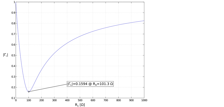
Figure 4. Reflection coefficient as a function of .
.
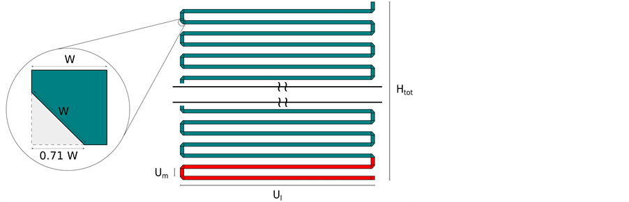
Figure 5. Detail of layout of the proposed folded microstrip delay-line.
The distance  had been determined through dedicated simulations in order to minimize the interaction between two neighbouring strips. In such simulations a simplified microstrip with four meanders is implemented, as shown in Figure 6, where the value of
  is progressively increased until the simulated scattering parameters values achieve the desired
  convergence level (that is the maximum expected variation due to
  of trace length mismatch). The number of meanders was set to four in order to enhance the effect of the neighbour strips interaction on the scattering parameters. The length of each meander finger is imposed to
  in order to make the final structure area possibly lower of that one occupied by inductors. The two termination branches are perpendicular to meander fingers in order to minimize their interaction with the meander itself. Their length
  decrease as the
  increases to maintain constant the total strip length according to
 (10)
(10)
If the condition in Equation (10) is not respected, the scattering parameters variation also depends on the  increasing the total effective strip length. Simulations on the model showed that the scattering parameters convergence occurs at
 .
.
The microstrip reported in Figure 5 has been sized in order to obtain the  delay between the input voltage maximum and the output current maximum of the PG. For this purpose, a circuital test-bench formed by a PG and two Thevenin equivalent generators has been simulated. These equivalents generators provide to model the tanks DC and fundamental behaviours at nodes
  and
and  including the observed impedance.
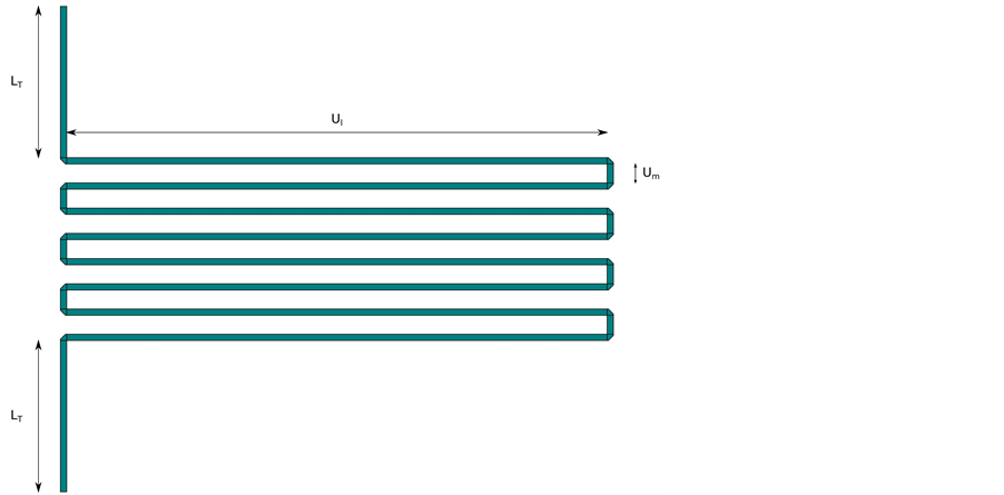
Figure 6. Simplified folded microstrip delay-line.
 (11)
(11)
The value of  is chosen less than
  of the
  in order to consider the saturation effect of the drivers
  into the fundamental signal amplitude.
  and
and  are the tank inductance and capacitance, respectively.
  is the observed parallel resistance at the resonance frequency
 .
.
The length of the microstrip is initially chosen by Equation (9). Progressive adjustments of the  lead to the proper positioning of the refilling current pulse on the test-bench. In this manner, a simulations loop has been created. The microstrip scattering parameters are calculated with CST Microwave Studio® and exported, through a Touchstone file, into SpectreRF® which in turn, simulating the test-bench, gives the indication to next adjustment step of the microstrip length
  into the 3D simulator. At the end of such process, to reach the desired delay a total length of the microstrip
  is needed. This length requires a number of
  meanders with
 . Furthermore, the microstrip area has been optimized to conform it in square shape by means of a dedicated routing algorithm. Finally the process variations regarding metallization levels involved in the delay-line design have been accounted with two corners, a short-line case and a long-line case with respect to the nominal length. The simulated variations on nominal scattering parameters for these two corners are evaluated in
 , a value close to the convergence level, thus, hereafter we consider them as negligible.
4. Simulation results and Literature Comparison
The oscillator has been implemented in the LFoundry  RF CMOS process with a tuning frequency range spanning the
  ISM band by a 4-bit digitally selectable capacitors bank. All the simulations were run with SpectreRF® simulator in Cadence® 6.1.5 environment. The inductance per branch of the center tapped inductor is
  whereas the fixed capacitance used to set the upper bound of the
  band is
 . The sizing of driver transistors following the Equation (4) results in a total of
  on
on , whereas the optimal sizing of the buffer transistors has been found in
  on
on . The adopted settling time is set in
  obtained via
  and
and . The proposed architecture is first compared to a reference voltage limited phase and quadrature differential VCO implemented with a replica of the PQPBO resonator and based on the architecture proposed in [9] without the top PMOS crossed pair. Then the results of PQPBO are compared to recent literature phase and quadrature oscillator built in state of the art CMOS technologies and running at similar frequencies.
In architecture proposed in [9] the coupling between the two oscillators is reached by the introduction of coupling transistors in parallel to the crossed pair transistors. The crossed pair transistors of reference quadrature VCO, indicated with , have total
  on
on  sizing, whereas coupling transistors, indicated as
 , have total
  on
on  sizing. The
  dimension has been chosen as the minimum width granting the effective quadrature. Process variations and mismatches of active devices dimensions of both proposed and reference oscillators play a negligible role, since all of them work in large signal condition (comprising the
  with a not so sensitive gate polarization voltage).
In the first comparison the oscillation amplitudes are kept at a fixed level of , whereas the maximum supply voltage for this technology
 .
.
In Figure 7 the transient PSS node voltages of  and
and  are reported for PQPBO running at
 . As can be inferred from Figure 7 and as it was measured by the frequency domain PSS results, the signals show
  oscillation amplitude level with an amplitude difference lower than
 , whereas the quadrature phase error is lower than
 .
.
In Figure 8 the transient PSS results of the phase relation between the  voltage driving the PG injecting current in tank node is reported. The phase displacement of driver current is calculated as
 . The quadrature error is lower than
 . However this phase re-
lation is not directly related to the overall quadrature phase error between the tank node voltages signals, since the receiving resonant tank undergoes to a pulling due to the whole current pulse rather than to the position of the peak only. This phenomenon results in an attenuation of the quadrature error of about an order of magnitude in phase degree, allowing the phase error between voltage signals to be lower than .
.
The phase noise results are presented in Figure 9 for VCOs running at  at nominal temperature of
 .
.
As expected from a pulsed bias architecture the phase noise improvement is consistent especially at low offsets. However, to avoid bias dependence on results, we set the comparison at  where white noise contributors dominate. The improvement is measured in
 . At lower offsets the phase noise improvement can be higher than
 . This can be explained considering that in the reference oscillator, in order to achieve the quadrature coupling on relative phases between resonators I and Q, the
  transistors inject a not negligible charge quantity in the oscillation portion more sensitive to phase variations. At offsets higher than
  the phase noise improvement drops, however we remark such high frequency offsets are not of concern for any of actual phase noise masks in ISM modulations. For a complete comparison we need to evaluate power consumption, calculated with
  as the product of
  supply voltage and the total DC current calculated by PSS analysis. Reference oscillator dissipates
  whereas the PQPBO reaches
  subdivided in
  and
and  for driver and buffer transistors, respectively. Such high efficiency is explained by the operation in C-class of the PQPBO.
 (12)
(12)
According to Figure of Merit in Equation (12), phase noise  is evaluated at
  with
with  obtaining
  for the reference oscillator and
  for the PBO. We conclude that a
  increment of
  is effectively observed at an offset frequency where white noise source dominate. The
  increment increases for lower offsets. Finally, the area of every delay line is
  and the total area of the two inductors is
 . Thus the four microstrips area occupation represents only the
  of the inductors area.
In the second comparison we gather a list of recently proposed phase and quadrature VCO architectures with both coupling based on active devices and on passive components. The results are reported in Table 1, showing that the proposed PQPBO may reach a state-of-the-art  with a very reduced quadrature error.
5. Concluding Remarks
In this paper a PQPBO based on a novel coupling method has been proposed. The coupling method adopts a delay-line implementation with an extremely compact meander microstrip structure. The design equations for the PQPBO, with a dedicated section on the DL optimization, have been pursued. The PQPBO has been implemented
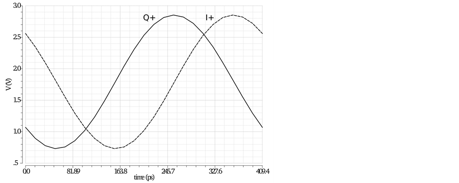
Figure 7. PSS transient result of  and
and  nodes voltage.
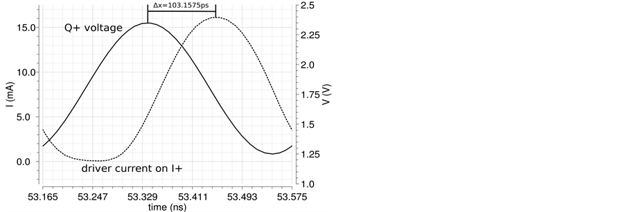
Figure 8. PSS transient result of  voltage (continuous line) driving the PG injecting current (dotted line) in tank node
 .
.
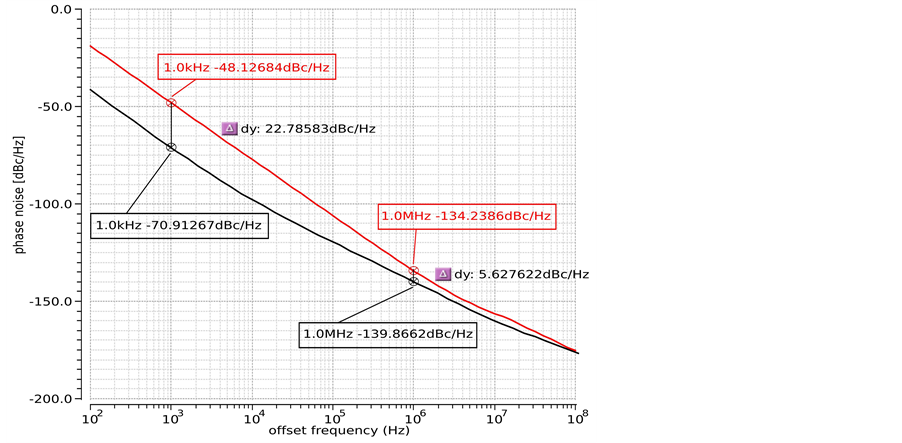
Figure 9. Phase noise results for the PQPBO (black trace) and for the refe- rence oscillator (red trace).

Table 1. Comparison with literature phase and quadrature VCOs.
at LVS level in a LFoundry  RF CMOS technology with a tuning frequency range spanning the
  showing a state-of-the-art
  compared to recent literature phase and quadrature VCOs with a very reduced quadrature error. These promising results encourage further optimization of the proposed architecture and an effective on-chip realization.
Cite this paper
FrancescoStilgenbauer,StefanoPerticaroli,FabrizioPalma, (2014) CMOS Phase and Quadrature Pulsed Differential Oscillators Coupled through Microstrip Delay-Lines. Circuits and Systems,05,181-190. doi: 10.4236/cs.2014.58020
References
- 1. Perticaroli, S., Luli, N. and Palma, F. (2011) Derivation of Floquet Eigenvectors Displacement for Optimal Design of LC Tank Pulsed Bias Oscillators. SCIRP Circuits and Systems, 2, 311-319.
http://dx.doi.org/10.4236/cs.2011.24043 - 2. Perticaroli, S., Palma, F. and Carbone, A. (2011) Phase and Quadrature Pulsed Bias LC-CMOS VCO. SCIRP Circuits and Systems, 2, 18-24.
http://dx.doi.org/10.4236/cs.2011.21004 - 3. Traversa, F.L. and Bonani, F. (2011) Oscillator Noise: A Nonlinear Perturbative Theory Including Orbital Fluctuations and Phase-Orbital Correlation. IEEE Transactions on Circuits and Systems I, 58, 311-319.
- 4. Carbone, A. and Palma, F. (2006) Considering Orbital Deviations on the Evaluation of Power Density Spectrum of Oscillators. IEEE Transactions on Circuits and Systems-II: Express Briefs, 53, 438-442.
- 5. Bizzarri, F., Brambilla, A., Perticaroli, S. and Gajani, G.S. (2011) Noise in a Phase-Quadrature Pulsed Energy Restore Oscillator. European Conference on Circuit Theory and Design (ECCTD), 465-468.
- 6. Bahl, I.J. (2003) Lumped Elements for RF and Microwave Circuits. Artech House, Norwood.
- 7. Gupta, K.C., Garg, R. and Bahl, I.J. (1996) Microstrip Lines and Slotlines. 2nd Edition, Artech House Inc., Norwood.
- 8. Douville, R.J.P. and James, D.S. (1978) Experimental Study of Symmetric Microstrip Bends and Their Compensation. IEEE Transactions on Microwave Theory and Techniques, 26, 175-182.
http://dx.doi.org/10.1109/TMTT.1978.1129340 - 9. Peng, K.C. and Lee, C.H. (2012) A 5 GHz CMOS Quadrature VCO with Precise Quadrature Phase. Microwave Conference Proceedings (APMC), Asia-Pacific, 1211-1213.
- 10. Torkzadeh, P., Atarodi, M. and Javidan, J. (2009) A Low Power, Low Phase Noise, Square Wave LC Quadrature VCO for ISM Band. Circuits and Systems and TAISA Conference, Toulose, 1-4.
- 11. Gierkink, S.L.J., Levantino, S., Frye, R.C., Samori, C. and Boccuzzi, V. (2003) A Low-Phase-Noise 5-GHz CMOS Quadrature VCO Using Superharmonic Coupling. IEEE Journal of Solid-State Circuits, 38, 1148-1154.
http://dx.doi.org/10.1109/JSSC.2003.813297 - 12. Huang, T.H. and Tseng, Y.R. (2008) A 1 V 2.2 mW 7 GHz CMOS Quadrature VCO Using Current-Reuse and Cross-Coupled Transformer-Feedback Technology. IEEE Microwave and Wireless Components Letters, 18, 698-700.
http://dx.doi.org/10.1109/LMWC.2008.2003477 - 13. Huang, G. and Kim, B.S. (2009) Low Phase Noise Self-Switched Biasing CMOS LC Quadrature VCO. IEEE Transactions on Microwave Theory and Techniques, 57, 344-351.
http://dx.doi.org/10.1109/TMTT.2008.2009901