Circuits and Systems
Vol.5 No.2(2014), Article ID:43169,6 pages DOI:10.4236/cs.2014.52006
A Domain Extension Algorithm for Digital Error Correction of Pipeline ADCs
1Electrical and Computer Engineering Department, North Dakota State University, Fargo, USA
2Information Engineering School, Nanchang University, Nanchang, China
Email: ting.li@my.ndsu.edu, you.chao@gmail.com
Copyright (c) 2014 Ting Li, Chao You. This is an open access article distributed under the Creative Commons Attribution License, which permits unrestricted use, distribution, and reproduction in any medium, provided the original work is properly cited. In accor-dance of the Creative Commons Attribution License all Copyrights (c) 2014 are reserved for SCIRP and the owner of the intellectual property Ting Li, Chao You. All Copyright (c) 2014 are guarded by law and by SCIRP as a guardian.
Received 6 January 2014; revised 6 February 2014; accepted 13 February 2014Keywords:Behavioral Simulation; Comparator Offsets; Domain Extension Algorithm; Pipeline ADCs
ABSTRACT
A domain extension algorithm to correct the comparator offsets of pipeline analog-to-digital converters (ADCs) is presented, in which the 1.5-bit/stage ADC quantify domain is extended from a three-domain to a five-domain. This algorithm is designed for high speed and low comparator accuracy application. The comparator offset correction ability is improved. This new approach also promises significant improvements to the spurious-free dynamic range (SFDR), the total harmonic distortion (THD), the signal-to-noise ratio (SNR) and the minor analog and digital circuit modifications. Behavioral simulation results are presented to demonstrate the effectiveness of the algorithm, in which all absolute values of comparator offsets are set to |3Vref/8|. SFDR, THD and SNR are improved, from 34.62-dB, 34.63-dB and 30.33-dB to 60.23-dB, 61.14-dB and 59.35-dB, respectively, for a 10-bit pipeline ADC.
1. Introduction ADCs are widely used in many areas, such as music recording, healthcare, radar systems and communication [1]. A trend of the modern ADC design is the use of digital background calibration to compensate for the raw performance of analog circuits [2-9]. However, many digital background calibrations can only correct gain errors [10,11], which are caused by finite op-amp gain and capacitor mismatches. This leaves the comparator offsets corrected by the traditional digital error correction technique or not corrected at all. The traditional 1.5- bit/stage ADC can only correct the comparator offsets within ± [12]. For small-geometry transistors, typical mismatches in the width, length and threshold voltage can lead to significant comparator offsets [13]. Comparator offsets greatly limit the accuracy of a switched capacitor pipeline ADC. In this paper, a new algorithm is developed to improve the comparator offset correction ability for the 1.5-bit/stage pipeline ADC. This innovative algorithm increases the comparator offset toleration ability by 50%. In addition, the algorithm also provides crucial information on both overflow and underflow situations.
2. Domain Extension Algorithm
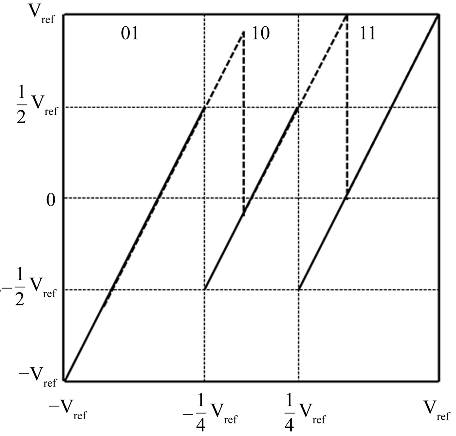
Figure 1(a) shows the residue plot of the traditional 1.5- bit/stage ADC. In Figure 1(a), two ideal threshold voltages are  and
and  shown with dotted lines. The coded range is from
  to
to . The residue plot of a real ADC with comparator offsets is shown using dashed lines. In this case, the maximum comparator offset is
  and the corresponding maximum output equals to
 . Since the output of the current stage is the input of the next stage, and the input range is from
  to
to , the out of range output leads to code loss. In order to prevent the ADC from code loss, the comparator offsets should be within the range of
 .
.
Figure 1(b) shows the residue plot of the proposed 1.5-bit/stage ADC. Here, the ideal threshold voltages are ,
,  ,
,  , and
, and . This coded
 (a)
(a)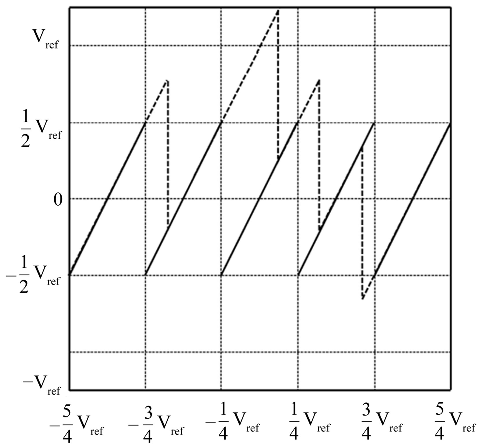 (b)
(b)
Figure 1. (a) Residue plot of the traditional 1.5-bit/stage ADC and (b) residue plot of the five-domain 1.5-bit/stage ADC.
range is from 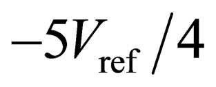 to
to . By adding two comparators with comparison voltages of
 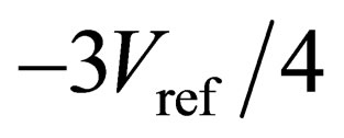 and
and  to the lower and upper sides of traditional 1.5- bit/stage ADC, the analog quantify domain is a five-domain rather than a three-domain; therefore, this proposed configuration is referred to as a five-domain 1.5-bit/stage ADC. Like in Figure 1(a), the residue plot of a real ADC with comparator offsets in Figure 1(b) is shown in the dashed lines. In this case, the maximum comparator offset is
 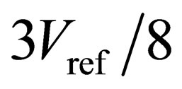 and the corresponding outputis
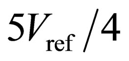 . Since the input range is changed to
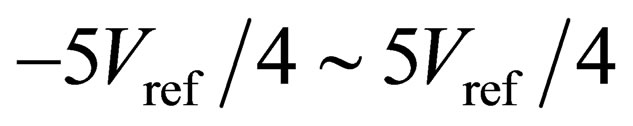 , the comparator offsets that the developed ADC can tolerate without code loss should be within the range of
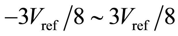 .
.
However, the traditional 1.5-bit/stage ADC can only correct the comparator offsets within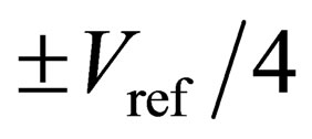 . In this research, a five-domain 1.5-bit/stage ADC is developed to increase the comparator offset correction ability to
 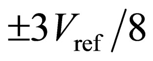 with an added overflow/underflow judgment. Two Matlab behavioral simulations are used to illustrate the improvement of the comparator offset correction ability for the proposed ADC. The first ADC behavioral simulation includes eight traditional 1.5-bit/stage converters followed by a flash ADC, and the second ADC behavioral simulation includes eight trial 1.5-bit/stage converters also followed by a flash ADC. In these simulations, the absolute values of the comparator offsets are set between 0 and
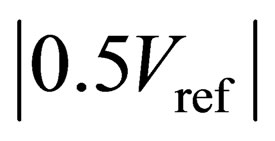 . In order to control and narrow research findings, all 1.5-bit/stage ADCs are onlycomplicated by the comparator offsets. In addition, the flash ADCs setting are ideal. In these simulations, the total number of conversions is
 . The total miscode numbers, and their related comparator offsets, are show in Figure 2. According to Figure 2, for the ADC based on the traditional digital error correction technique, miscodes occur when the absolute values of the comparator offsets are higher than
 . By comparison, no miscodes occur for the absolute values of the comparator offsets lower than
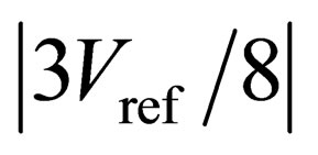 , for the ADC based on the proposed algorithm.
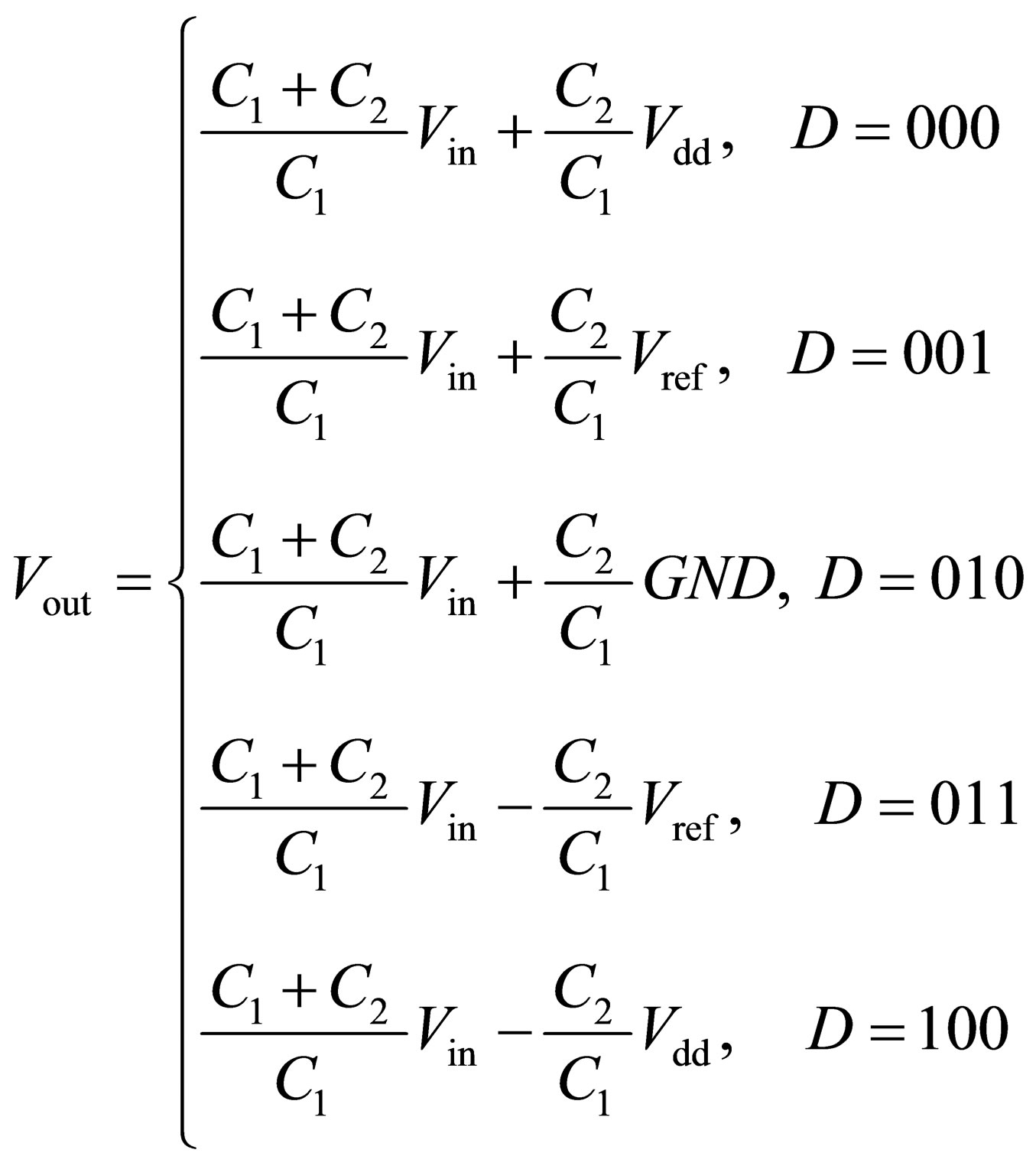
The transfer function of the traditional 1.5-bit/stage pipeline ADC is given by the following equation [14]:
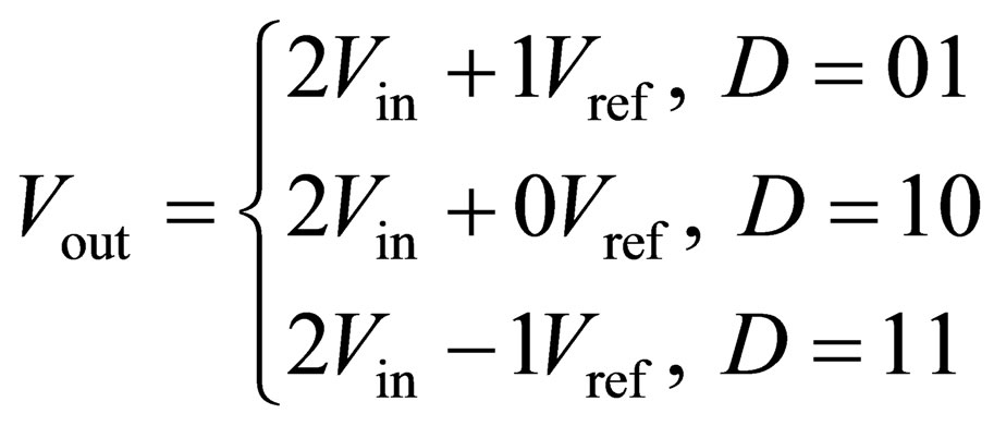 . (1)
. (1)
The transfer function of the proposed five-domain 1.5- bit/stage pipeline ADC is given by the following equation:
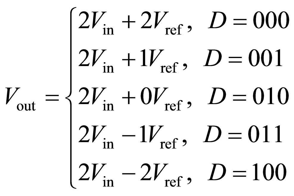 . (2)
. (2)
This proposed ADC consists of eight 1.5-bit stages followed by a 2-bit flash ADC. There are 12 total output bits, 10usable bits and the first two bits are utilized as overflow/underflow bits. Figure 3 shows the algorithm process. In order to have the digital output of five-domain 1.5-bit/stage ADC consistent with the traditional 1.5-bit/stage ADC, the subtraction of one operation is needed. Since 000 minus 1 is negative, adding a “1” in front of the digital output of the first stage avoids the negative number. For the same reason, the later stages also need to subtract one operation. In addition, the dislocation addition should be implemented before the subtraction of one. The first two bits are overflow/underflow bits. Therefore, when they are “11” or “01”, they will reference to the input signal beyond or below the reference
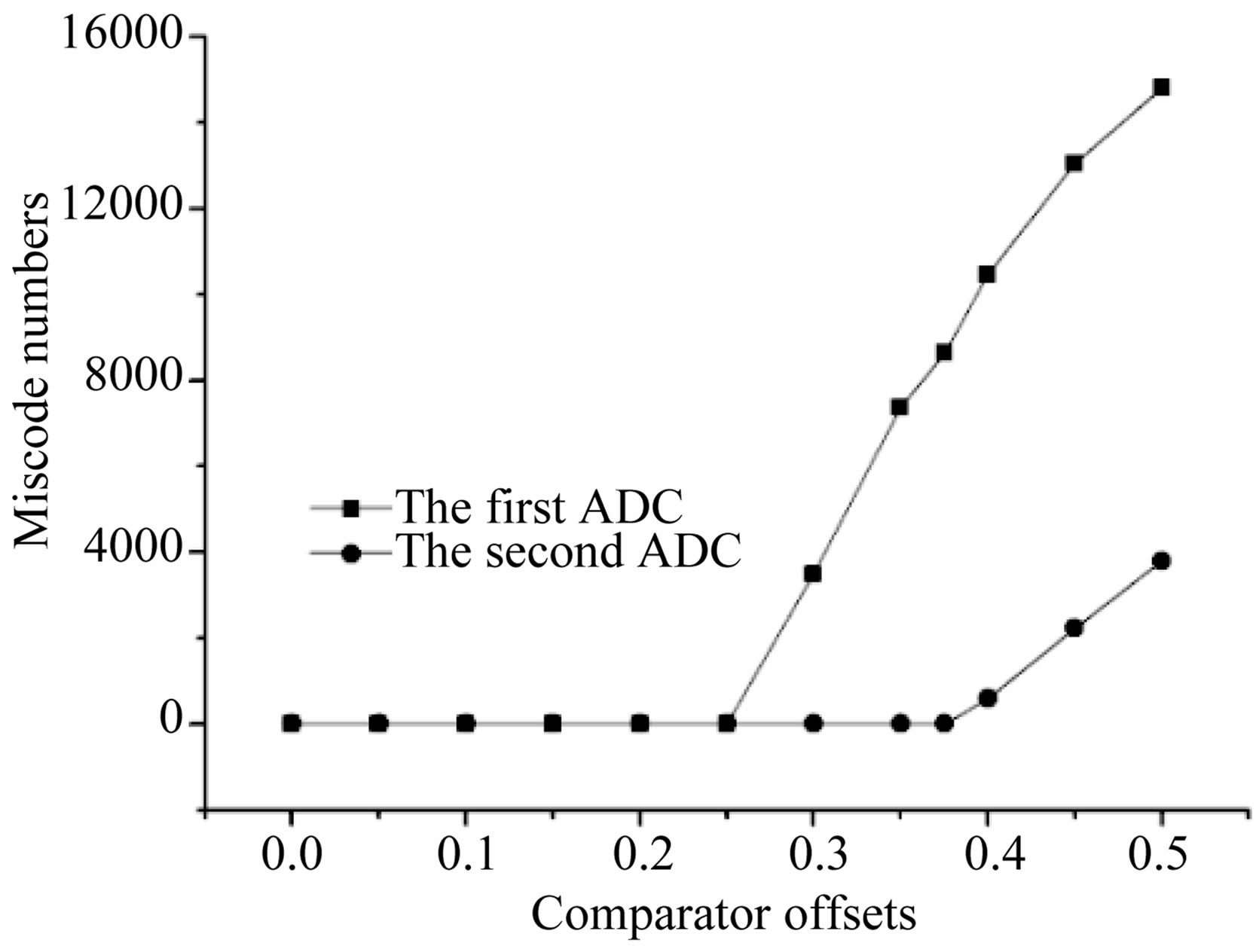
Figure 2. Miscode numbers for various comparator offsets.
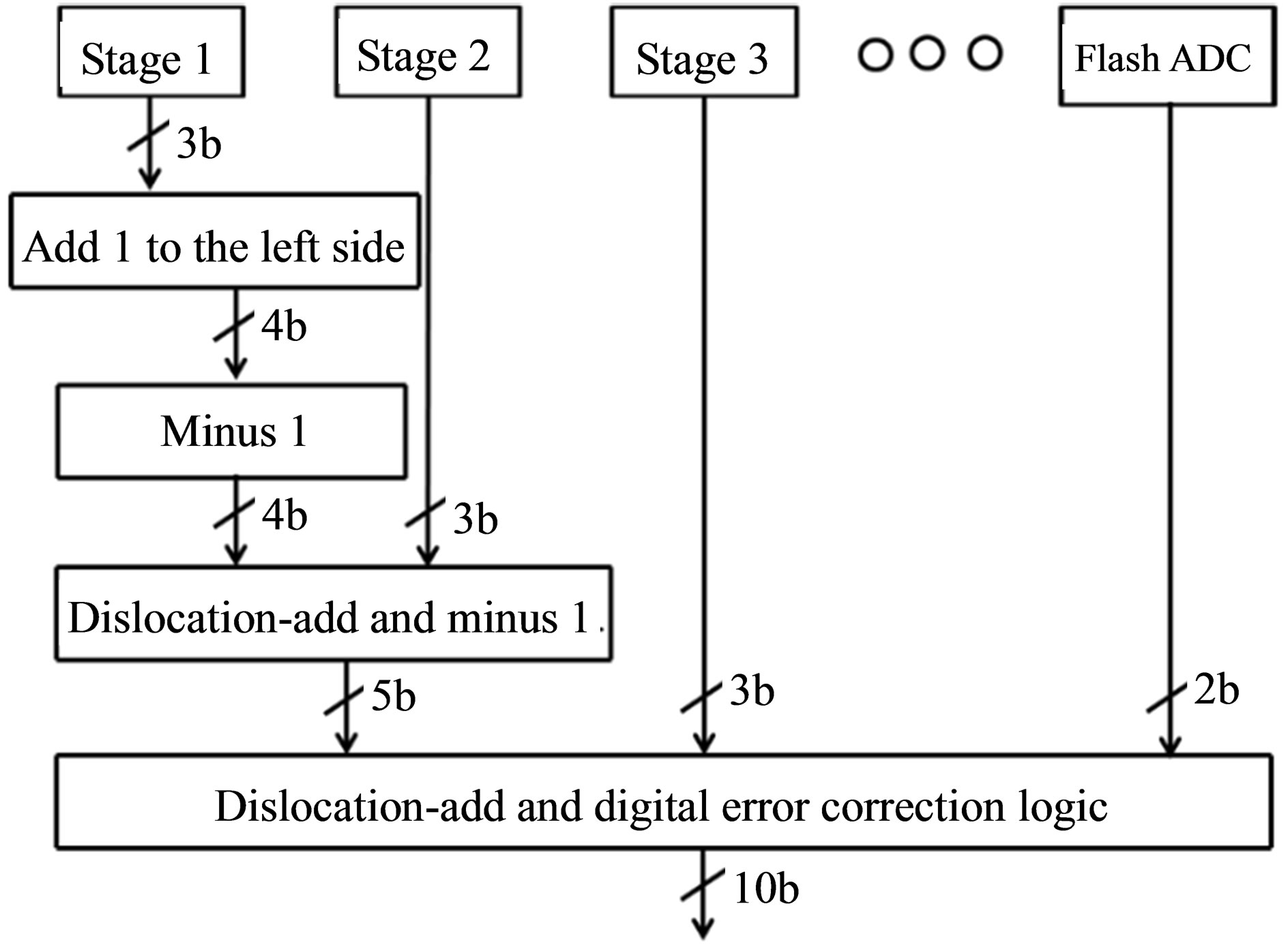
Figure 3. Five-domain 1.5-bit/stage ADC algorithm process.
range; otherwise when they are “10”, the remaining ten bits are usable digital output bits.
The proposed algorithm of the ADC, shown in Figures 4(a) and 4(b), uses  of 1 V and the input voltage of 0.4 V. The traditional algorithm is shown in Figures 4(c) and 4(d) uses the same
  and input values. To prevent the influences from flash-ADCs, all of the threshold voltages are set to be the ideal. In Figure 4(a), the absolute values of comparator offsets are set to be
 . In this case, for the first eight stages, the threshold voltages are
 ,
,
 ,
,  , and
, and 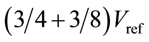 for all of the comparators. The first two bits are “10” indicating that the remaining ten bits are usable output codes. In Figure 4(b), all the comparators do not suffer from comparator offsets. Figure 4(c) shows the processing of output codes based on the traditional digital error correction technique with the comparator offsets the same as Figure 4(a), but the threshold voltages are
  and
and . Figure 4(d) shows the processing of output based on the traditional technique with the comparator offsets set to be zero. These three cases, Figures 4(a), 4(b), and 4(d), have the correct digital output, while Figure 4(c) is different from the other three because the traditional technique cannot correct the absolute values of comparator offsets higher than |Vref/4|.
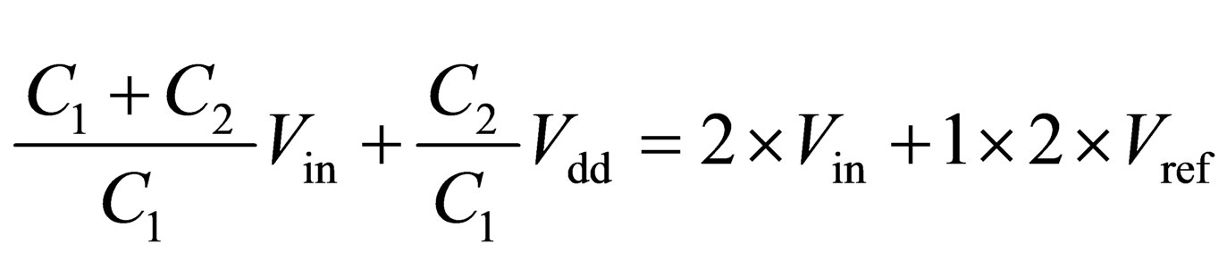
The circuit level implementation of Equation (2) is given by
 (3)
(3)
In Equation (3), the two capacitors are equal. When the required gain is one, the circuit level realization is the same as the traditional technique, and capacitor  connects to the corresponding reference voltage. However, a gain of two for
  cannot be realized through the traditional technique since one of the capacitors is the feedback capacitor. The maximum gain for
  is the non-feedback capacitor divided by the feedback capacitor, which is one. To extend the domain, a new method is proposed. In this new method
  need to be set to twice the
 . The first and the last equations of (3) are
 . (4)
. (4)
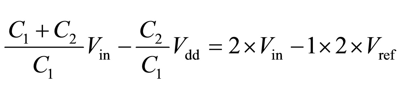 . (5)
. (5)
Figures 5(a) and 5(b) are the circuit configurations based on the traditional technique and the proposed algorithm, respectively.  is simplified by
 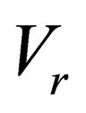 in the figures. Although the actual configurations are fully differential, the sing-ended the configurations are shown for simplicity. When
  is high, the converters work on the sample phase, input is sampled on the two capacitors simultaneously. When
 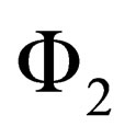 is high, they work on the amplification phase, the feedback capacitor
  connects to the output and the non-feedback capacitor
  connects to the corresponding reference voltage.
The proposed algorithm slightly modifies the analog. Two comparators are added to extend the quantify domains, and two references are used to provide a gain of two for . Since the actual configuration is fully dif-
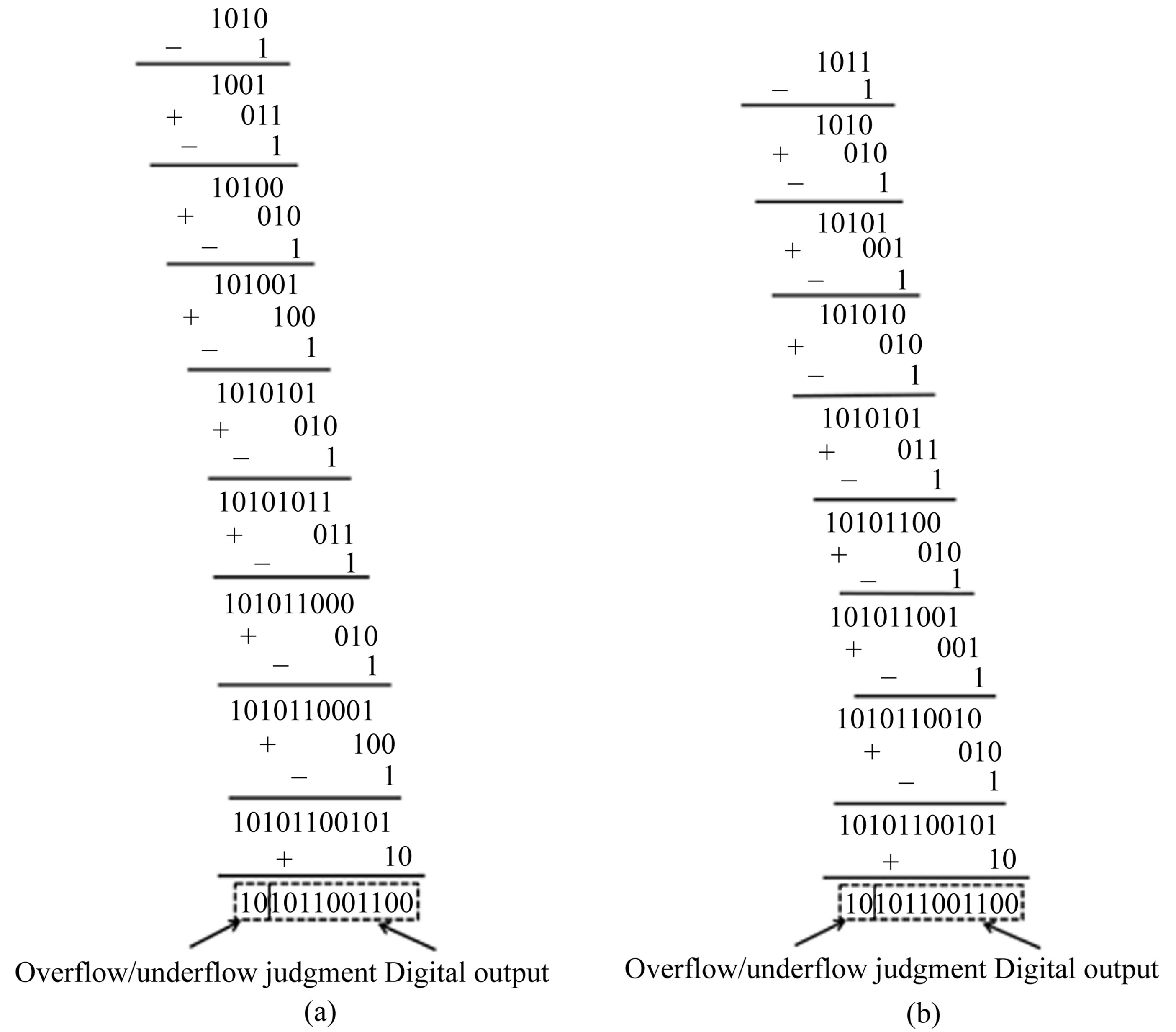
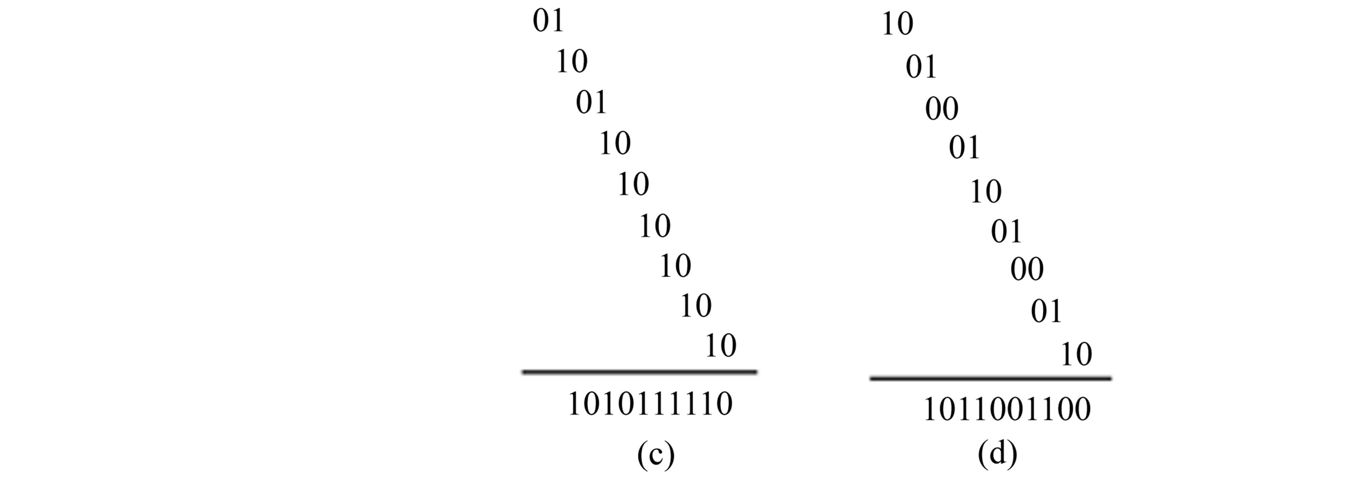
Figure 4. (a) Example of the proposed algorithm with the comparator offset of 3Vref/8; (b) Example of the proposed algorithm with no comparator offset; (c) Example of the traditional algorithm with the comparator offset of 3Vref/8; (d) Example of the traditional algorithm with no comparator offset.
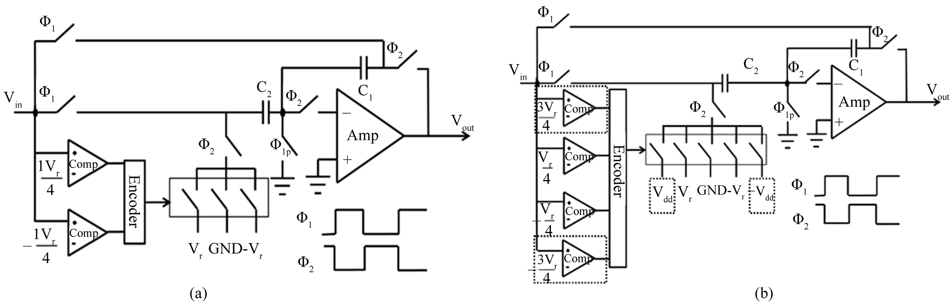
Figure 5. (a) Circuit implementation based on the traditional 1.5-bit/stage ADC and (b) Crcuit implementation based on the five-domain 1.5-bit/stage ADC.
ferential,  can be realized by connecting the ground to the positive input side of the amplifier and the
  to the negative input side of the amplifier in both configurations. The realization of
  is similar to the realization of
 . In the digital domain, only several dislocation and subtraction blocks need to be added.
3. Simulation Results
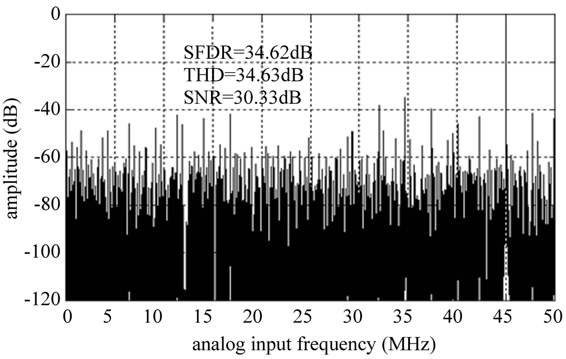
In order to demonstrate the effectiveness of the domain extension algorithm, a 10-bit pipeline ADC was simulated in MATLAB. The ADC consisted of eight fivedomain 1.5-bit/stage converters and a 2-bit flash ADC. In the simulation, all absolute values of comparator offsets were set to , input frequency was set to 45-MHz, and sample rate was set to 100-MS/s. The Fast Fourier Transform (FFT) plot of this simulation using the traditional method is shown in Figure 6(a). The dynamic performance as shown in the FFT plot is recorded as 34.62-dB SFDR, 34.63-dB THD, and 30.33-dB SNR. Figure 6(b) shows the FFT plot using the domain extension algorithm. In this case, the ADC achieves a dynamic performance of 60.23-dB SFDR, 61.14-dB THD, and 59.35-dB SNR. The resulting improvements are then 25.61-dB, 26.51-dB, and 29.02-dB for SFDR, THD, and SNR respectively.
The simulated dynamic performance of the ADCs at an 100-MS/s sample rate and a 45-MHz input frequency is summarized in Figure 7. The absolute values of the comparator offsets are from 0 to . As shown in Figure 7(a), SFDR, THD, and SNR decrease minimally from the low comparator offsets to the absolute values of comparator offsets of
 . However, they decrease significantly when the absolute values of comparator offsets are higher than
 , because the traditional digital error correction technique can only correct the absolute values of compactor offsets lower than
 . As shown in Figure 7(b), SFDR and THD decrease minimally from the low comparator offsets to the absolute values of comparator offsets of
 , because the lease significant bit (LSB) cannot be corrected and the bit error rate (BER) increases with the increased comparator offsets.
 (a)
(a)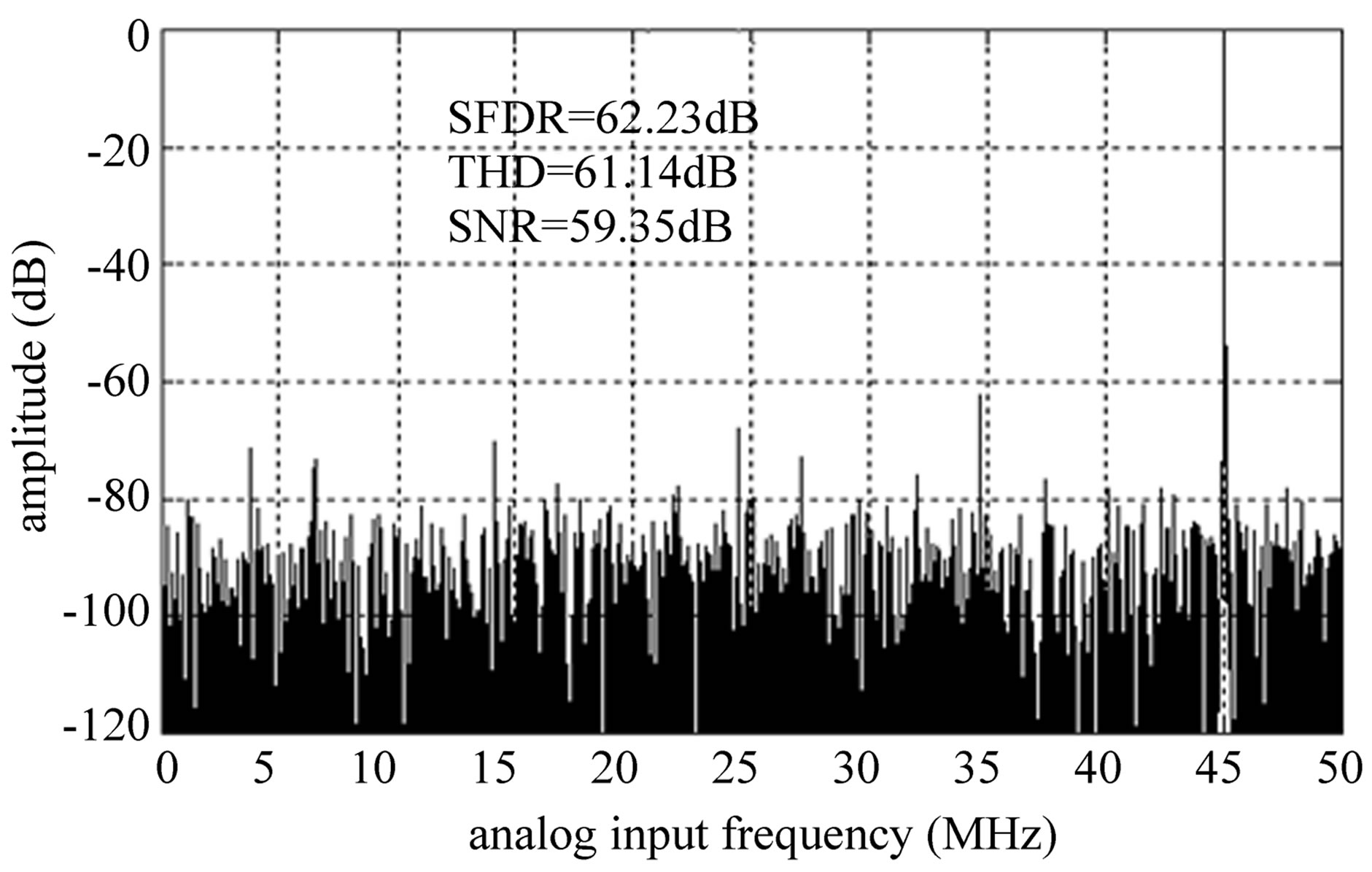 (b)
(b)
Figure 6. FFT plots of a 10-bit pipeline ADC using (a) the traditional digital error correction technique and (b) the proposed algorithm.
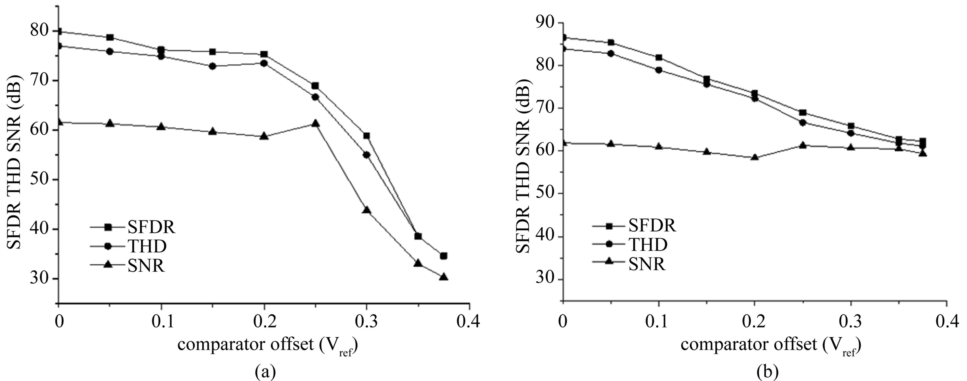
Figure 7. Simulated dynamic performance using (a) the traditional digital error correction technique and (b) the proposed algorithm.
4. Conclusion
The decrease of the transistor geometry causes problematic mismatches in width, length and threshold voltage, which leads to significant comparator offsets. These comparator offsets, in turn, greatly limit the performance of ADCs. However, the traditional digital error correction technique can only correct the absolute value of comparator offsets lower than . Therefore, in order to improve the comparator offset toleration ability, a domain extension algorithm has been presented, which can correct the absolute value of comparator offsets within
 . This new approach involves minor analog and digital modifications and increases the comparator offset toleration ability by 50% with overflow/underflow judgment. Simulation results have revealed significant improvements of SFDR, THD and SNR performance.
REFERENCES
- B. Peng, H. Li, P. Lin and Y. Chiu, “An Offset Double Conversion Technique for Digital Calibration of Pipelined ADCs,” IEEE Transactions on Circuits and Systems-II: Express Briefs, Vol. 57, No. 12, 2010, pp. 961-965.
- C. Tsang, Y. Chiu, J. Vanderhaegen, S. Hoyos, C. Chen, R. Brodersen and B. Nikolic, “Background ADC Calibration in Digital Domain,” Proceedings of IEEE Custom Integrated Circuits Conference, San Jose, 21-24 September 2008, pp. 301-304.
- Y. Chiu, C. W. Tsang, B. Nikolic and P. R. Gray, “Least Mean Square Adaptive Digital Background Calibration of Pipelined Analog-To-Digital Converters,” IEEE Transactions on Circuits and Systems I: Regular Papers, Vol. 51, No. 1, 2004, pp. 38-46. http://dx.doi.org/10.1109/TCSI.2003.821306
- W. Liu, P. Huang and Y. Chiu, “A 12b 22.5/45MS/s 3.0 mW 0.059 mm2 CMOS SAR ADC Achieving over 90 dB SFDR,” Proceedings of IEEE ISSCC Digest of Technical Papers, San Francisco, 7-11 February 2010, pp. 380-382.
- J. McNeill, M. C. W. Coln and B. J. Larivee, “‘Split ADC’ Architecture for Deterministic Digital Background Calibration of a 16-Bit 1-MS/s ADC,” IEEE Journal of SolidState Circuits, Vol. 40, No. 12, 2005, pp. 2437-2445. http://dx.doi.org/10.1109/JSSC.2005.856291
- J. Li and U.-K. Moon, “Background Calibration Techniques for Multistage Pipelined ADC’s with Digital Redundancy,” IEEE Transactions on Circuits and Systems II, Analog & Digital Signal Processing, Vol. 50, No. 9, 2003, pp. 531-538.
- J. A. McNeill, S. Goluguri and A. Nair, “‘Split ADC’ Digital Background Correction of Open-Loop Residue Amplifier Nonlinearity Errors in a 14b Pipeline ADC,” Proceedings of IEEE ISCAS, New Orleans, 27-30 May 2007, pp. 1237-1240.
- L.-H. Hung and T.-C. Lee, “A Split-Based Digital Background Calibration Technique in Pipelined ADCs,” IEEE Transactions on Circuits and Systems-II: Express Briefs, Vol. 56, No. 11, 2009, pp. 855-859.
- M. Taherzadeh-Sani and A. A. Hamoui, “Digital Background Calibration of a 0.4-pJ/step 10-Bit Pipelined ADC without PN Generator in 90-nm Digital CMOS,” Proceedings of IEEE Asian Solid-State Circuits Conference, Fukuoka, 3-5 November 2008, pp. 53-56.
- J. P. Keane, P. J. Hurst and S. H. Lewis, “Background Interstage Gain Calibration Technique for Pipelined ADCs,” IEEE Transactions on Circuits and Systems I: Regular Papers, Vol. 52, No. 1, 2005, pp. 32-43. http://dx.doi.org/10.1109/TCSI.2004.839534
- S. Yang, J. Cheng and P. Wang, “Variable-Amplitude Dither-Based Digital Background Calibration Algorithm for Linear and High-Order Nonlinear Error in Pipelined ADCs,” Microelectronics Journal, Vol. 41, No. 7, 2010, pp. 403-410. http://dx.doi.org/10.1016/j.mejo.2010.04.012
- H. S. Lee, “A 12-b 600 ks/s Digitally Self-Calibrated Pipelined Algorithmic ADC,” IEEE Journal of Solid-State Circuits, Vol. 29, No. 4, 1994, pp. 509-515. http://dx.doi.org/10.1109/4.280701
- B. Razavi and B. A. Wooley, “A 12-b 5-Msample/s TwoStep CMOS A/D Converter,” IEEE Journal of Solid-State Circuits, Vol. 27, No. 12, 1992, pp. 1667-1678. http://dx.doi.org/10.1109/4.173092
- S. Hamami, L. Fleshel and O. Yadid-Pecht, “CMOS Image Sensor Employing 3.3V 12 Bit 6.3 MS/s Pipelined ADC,” Sensors and Actuators, Vol. 135, No. 1, 2007, pp. 119-125. http://dx.doi.org/10.1016/j.sna.2006.06.041