Journal of Modern Physics
Vol. 4 No. 9A (2013) , Article ID: 37408 , 7 pages DOI:10.4236/jmp.2013.49A001
Proposal on Tunneling Effect between Quantum Hall States
Kyokugen (Center for Quantum Science and Technology under Extreme Conditions), Osaka University, Toyonaka, Osaka, Japan
Email: sasaki@ns.sist.ac.jp
Copyright © 2013 Shosuke Sasaki. This is an open access article distributed under the Creative Commons Attribution License, which permits unrestricted use, distribution, and reproduction in any medium, provided the original work is properly cited.
Received July 23, 2013; revised August 26, 2013; accepted September 22, 2013
Keywords: Quantum Hall Effect; Tunneling Effect; ac-Josephson Effect
ABSTRACT
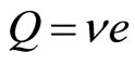
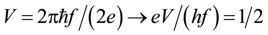
In the integer and fractional quantum Hall effects, the electric current flows through a thin layer under the strong magnetic field. The diagonal resistance becomes very small at integer and specific fractional filling factors where the electron scatterings are very few. Accordingly the coherent length is large and therefore a tunneling effect of electrons may be observed. We consider a new type of a quantum Hall device which has a narrow potential barrier in the thin layer. Then the electrons flow with tunneling effect through the potential barrier. When the oscillating magnetic field is applied in addition to the constant field, the voltage steps may appear in the curve of voltage V versus electric current I. If the voltage steps are found in the experiment, it is confirmed that the 2D electron system yields the same phenomenon as that of the ac-Josephson effect in a superconducting system. Furthermore the step V is related to the transfer charge Q as V = (hf)/Q where f is the frequency of the oscillating field and h is the Planck constant. Then the detection of the step V determines the transfer charge Q. The ratio Q/e (e is the elementary charge) clarifies the origin of the transfer charge. Many conditions are required for us to observe the tunneling phenomenon. The conditions are examined in details in this article.
1. Introduction
The value of the diagonal resistance is almost zero at integer quantum Hall (IQH) state [1]. This fact indicates that the scatterings of electrons by lattice vibrations and impurities are few in an IQH state. For the fractional quantum Hall (FQH) states with specific filling factors 1/3, 2/3 etc., the diagonal resistance is also almost zero [2,3]. This property makes it possible to observe a tunneling effect in a quantum Hall device.
In the previous paper [4], we proposed a new quantum Hall experiment where we observe the tunneling effect between two quantum Hall states in a device with the narrow potential barrier in the electron channel. The device proposed in the article [4] is shown in Figure 1. This old type of the device has some difficulties as will be examined below. So we improve it and propose a new type of the device which is illustrated in Figure 2.
The improved points are well seen by comparing Figure 2 with Figure 1. There are four potential probes A, B, C, D and four Hall probes a, b, c, d in Figure 2. The probes B, C, b, c are missing in the old type of the device in Figure 1. Accordingly in the old type of the device, we couldn’t detect the two diagonal resistances of the two areas separated by the narrow insulating region (potential barrier) in the middle of the conducting layer. Furthermore there is only one gate in the old type of the device. Therefore we couldn’t independently control the voltages of the two areas separated by the potential barrier. These imperfections are compensated in the new device of Figure 2.
The new device has the four potential probes A, B, C and D and therefore the diagonal resistance of the left area of the potential barrier is determined by (voltage between probes A and B)/(current) and also that of the right area is determined by (voltage between probes C and D)/(current). Furthermore we can independently control two voltages of the left and right areas by adjusting the voltages of the Gates 1 and 2, respectively.
We consider how to construct the potential barrier in the middle of the conducting layer on 2D electron system. Three types of the method are examined below.
Figure 2 shows the potential barrier with Type 1.
(Type 1) A narrow insulating region is inserted in the middle of the conducting layer as in Figure 2. The insulating region should have a width smaller than 2 nm to realize a tunneling effect. It would not be easy to fabricate this type of a device. Accordingly we consider the other types of a new device in order to fabricate more easily than Type 1.
(Type 2) The second type of quantum Hall device is illustrated in Figure 3 where there is a new gate (Gate 0). We can set an appropriate potential barrier by adjusting the voltage of the Gate 0. It would be easier to fabricate a device with Type 2 than Type 1.
One more type of a new device is illustrated in Figure 4 which is named Type 3.
(Type 3) The central part of the electron channel has an ultra-thin structure. The enlarged side view is illustrated in Figure 4, where the two quasi-2D electron systems are connected through the ultra-thin part. This type of junction is a familiar one in the superconducting quantum interference device (SQUID). When the electric current exceeds some critical value, this ultra-thin part plays a role of potential barrier. A device with this type can be made more easily than Type 1.
In the next section, we investigate the tunneling effect from the left area to the right area through the narrow potential barrier. Section 4 is devoted to examine the conditions which are required to yield the tunneling phenomenon like the ac-Josephson effect.
2. Tunneling Effect between Two Quantum Hall Sates
Using the devices shown in Figures 2-4, we propose to observe a tunneling effect in IQH or FQH state. This experiment is carried out as follows:
1) Magnetic field is applied in the direction perpendicular to the quasi-2D electron system as in Figures 2- 4. The strength of the applied magnetic field is adjusted to yield an IQH or an FQH state. Furthermore the filling factor in the left area of the potential barrier is set to be the same as that in the right area by adjusting the voltages of the Gates 1 and 2.
2) Next, an oscillating magnetic field is superposed on the static magnetic field. We may apply a periodic current modulation in addition to the constant current instead of an oscillating magnetic field. The frequency of the oscillation is described by f.
3) Thereafter we measure the voltage  between the potential probes B and C versus electric current I along the x-direction in Figures 2-4. The observation of
  curve is expected to give us interesting phenomena of the tunneling effect between the quantum Hall states.
When the electric current flows through the narrow potential barrier, the quasi-particle tunnels from the higher energy position to the lower one accompanying a stimulated emission of photon. This tunneling phenomenon is schematically drawn in Figure 5.
The stimulated emission is induced by the ac magnetic field with the frequency f. The emitted photon has the energy  where
where  is the Planck constant. At the same time the energy of the quasi-particle decreases by the value
  via the tunneling where the symbol Q indicates the electric charge of the quasi-particle. Because the total energy is conserved in this tunneling

Figure 1. An old type of the device proposed in the article [4]. There are one gate, two Hall probes and two potential probes.

Figure 2. (Type 1) Improved device with a narrow insulating area in the middle of thin layer. There are two gates, four Hall probes and four potential probes.
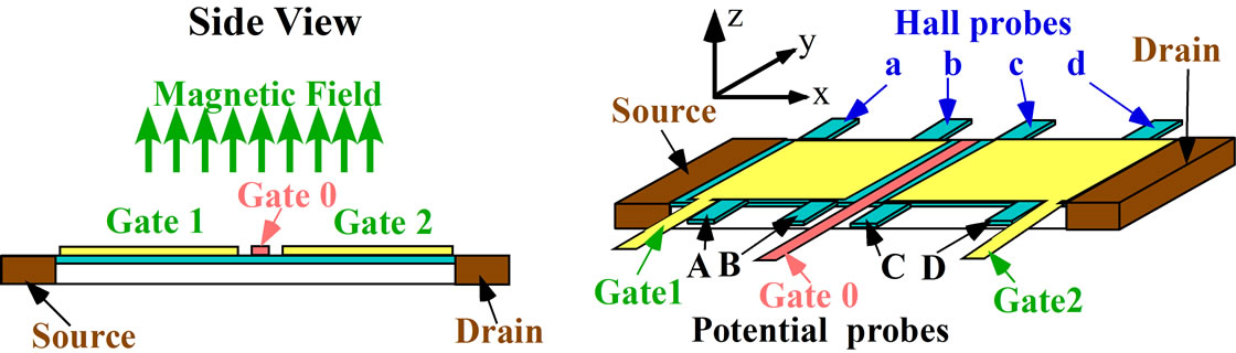
Figure 3. (Type 2) A device with a central Gate 0 creating the potential barrier.
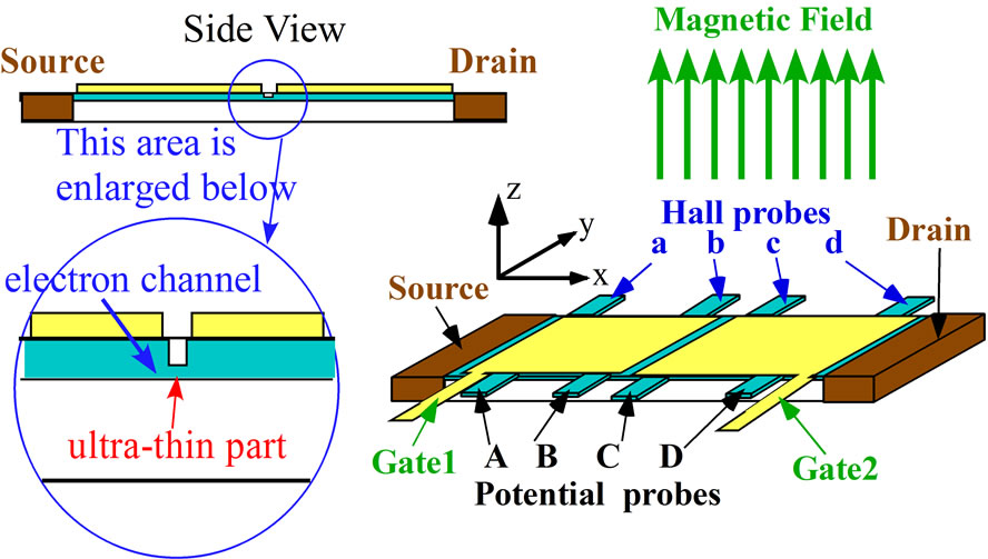
Figure 4. (Type 3) A device with ultra-thin structure. The ultra thin part yields the potential barrier when the current exceeds a critical value.

Figure 5. Tunneling phenomenon of quasi-particle beyond a potential barrier.
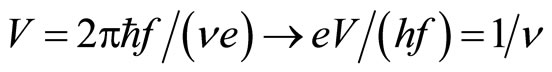
phenomenon, the voltage V is given by
 (1)
(1)
When the electric current becomes large, the stimulated emission yields multi-photons. Then the measured voltage becomes n times V as follows:
 (2)
(2)
Accordingly many voltage steps appear in the  curve.
In this experiment it is required that the diagonal resistances in both sides of the potential barrier are nearly equal to zero. The vanishings are confirmed by detecting the two voltages  and
and  which are detected between potential probes A and B, and between C and D, respectively. The voltages
  and
and  are required to be nearly equal to zero. Also the Hall voltage
  between probes B and b is required to be equal to
  between probes C and c, because the filling factors in both sides of the potential barrier should be the same as each other.
It is necessary that these conditions are satisfied during the whole measurement by adjusting the voltages of Gates 1 and 2. This phenomenon is reminiscent of the acJosephson effect. We discuss the  curve for the two cases namely IQHE and FQHE in the next section.
3. Behaviour of the Voltage versus Current in the Tunneling Effect of QHE
The voltage  between two potential probes B and C depends upon the electric current I from the source to the drain. Observation of
  curve gives us important information for the tunneling effect in the quantum Hall states. The stimulated emission creates the voltage steps as examined in Equations (1) and (2). The function form of
 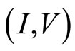 is studied for the following two cases (IQHE and FQHE).
Case A: Integer quantum Hall state
The integer quantum Hall effect is caused by discrete eigen-energy levels (Landau levels), where the Landau sate is created by an electron. Therefore the charge of the quasi-particles across the potential barrier is the elementary charge e. In this case, the theoretical  curve behaves as shown in Figure 6.
Case B: Fractional quantum Hall state
R. B. Laughlin introduced a quasi-particle with fractional electric charge and proposed a trial wave function [5,6]. The quasi-particles have fractional charges and obey fractional statistics [7-10]. Laughlin’s theory suggests that the charge of the quasi-particles across the potential barrier is  at the fractional number
 . We call it Case B-1.
(Case B-1) The theory with fractional charge (Laughlin’s theory):
 (3a)
(3a)
 (3b)
(3b)
Thus the value of the voltage step changes with the filling factor . For example
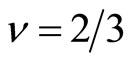 , the
, the  curve of Laughlin theory is shown in the left panel of Figure 7.
Next we examine the composite fermion model introduced by J. K. Jain [11,12] and developed by many physicists [13,14]. The composite fermion consists of an

Figure 6. (Case A) Integer quantum Hall effect. Electric current flows along the x-direction as shown in Figures 2-4.
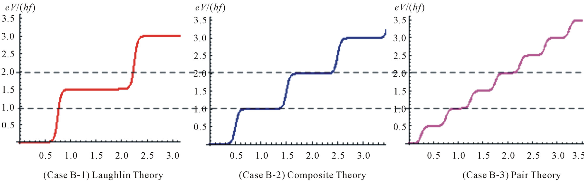
Figure 7. Behaviours of voltage steps for three theories at the filling factor 2/3. The horizontal axis indicates the electric current (arbitrary unit).
electron bound to an even number of magnetic flux quanta. Therefore the composite fermion has the elementary charge. That is to say the charge of the quasi-particles across the potential barrier is e at any filling factor . We call it Case B-2.
(Case B-2) Composite fermion theory:
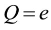 (4a)
(4a)
 (4b)
(4b)
The theoretical  curve of composite fermion theory is shown in the middle panel of Figure 7.
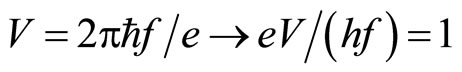
The present author has developed a theory based on the electron pair to explain the fractional quantum Hall effect [15-21]. The Coulomb interaction acts between electron pair and depends upon only the relative coordinate. Therefore the total momentum of the interacting electron pair conserves along the x-direction of Figures 2-4 via the Coulomb transition. The electron pair has a large binding energy at the specific filling factors where the number of the allowed Coulomb transitions becomes maximum [15-21]. Then the binding of the electron pairs is so strong that the pairing is expected to be held in the tunneling process. Accordingly the charge of the quasiparticles across the potential barrier should be equal to 2e. We call it Case B-3.
(Case B-3) Pair theory:
 (5a)
(5a)
 (5b)
(5b)
The theoretical  curve of the electron pair theory is shown in the right panel of Figure 7.
The theoretical  curves are different from each other among the three theories mentioned above. The theoretical curves are shown in Figure 7 at the filling factor 2/3. Therein the difference between them is clear by comparing the three panels with the others. Thus this proposal plays an important role to clarify the properties of FQH states. In order to find the stair-like curve, the following seven conditions should be satisfied which will be discussed in the next section.
4. Conditions for Observing Tunneling Effect between Quantum Hall States
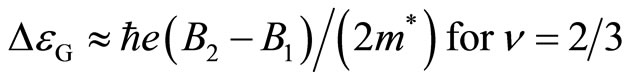
We study the excitation energy of the quantum Hall states. The Landau level energy EL is given by
 where L is the Landau level number
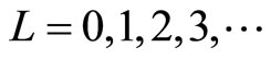 . When an electron in the IQH state with the Landau level L is excited to the higher Landau level
 , the excitation energy is given by
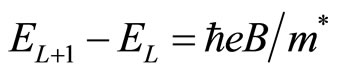
where  is the effective mass. The effective mass
  differs from material to material [22-24] and the value in GaAs is about 0.067 times the free electron mass.
For example this excitation energy is estimated for the experimental data [3] where the magnetic field strength is about 4T at the filling factor 
 . Then
 (6)
(6)
Thus the Landau excitation energy is very large. We next examine the excitation energy of FQH states. Figure 8 shows the diagonal resistance which is measured by W. Pan, H. L. Stormer, D. C. Tsui, L. N. Pfeiffer, K. W. Baldwin, and K. W. West [3].
Therein the filling factor is confined to  in the region of
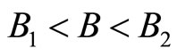 . Accordingly the FQH state with
  is stable in this region. The Landau energy increases from
 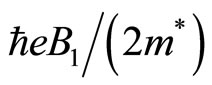 to
to 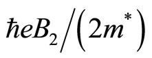 for
for  when the magnetic field increases from
  to
to . That

Figure 8. Diagonal resistance in FQHE [3].
is to say, the FQH state with  is stable for the increasing energy
 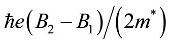 and therefore the excitation energy of
  is nearly equal to
 (7)
(7)
We estimate the value  for an example of the experiment [3]:
 (8)
(8)
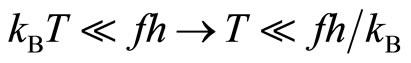
In order to maintain the ground state at , the frequency of the oscillating magnetic field should be smaller than
 .
.
(Condition 1)
The value of fh is set to be much smaller than the energy gap of the FQH state as,
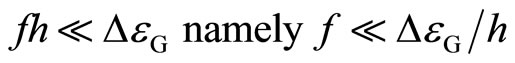 (9)
(9)
For example,  is about 62.7 GHz at
  in the experiment [3] as estimated in Equation (8). Because the value
 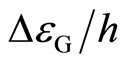 varies from sample to sample, the frequency f should be chosen to be appropriate for each device used in the tunneling experiment. When we apply f = 10 GHz as an example, the voltage step is 62.07 µV for the Case B-1, 41.38 µV for the Case B-2, and 20.69 µV for the Case B-3 respectively.
(Condition 2)
The thermal excitation energy should be lower than the energy 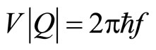 in the tunneling process.
 (10)
(10)
where T is the temperature and  is the Boltzmann constant. In the case of f = 10 GHz,
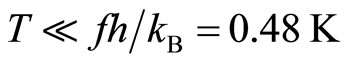 (11)
(11)
Accordingly the temperature should be cooled lower than a few 10 mK in this example.
(Condition 3)
Figure 9 shows the top view of the device. The current flows along the x-direction and the Hall voltage yields along the y-direction as seen in Figure 9 (see also Figures 2-4).
The diagonal resistances ,
,  in the left and right area of the potential barrier are required to be nearly equal to zero, in order to decrease the electron scatterings. The vanishings of
  and
and  are observed by detecting the voltages
  and
and , respectively. So the following conditions are required as:
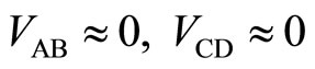 (12)
(12)
(Condition 4)
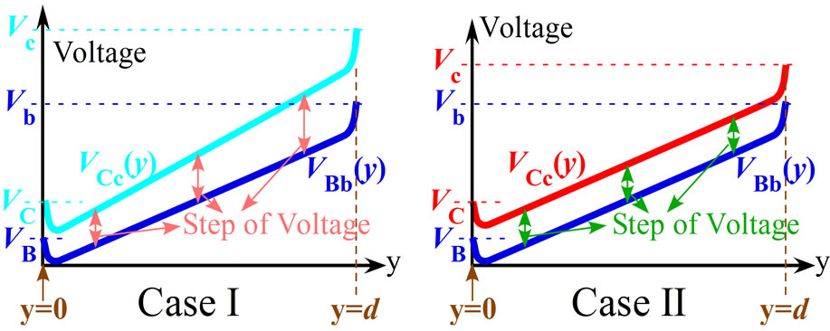
The Hall voltage of the left side of the potential barrier is measured between the probes B and b. Also that of the right side is measured between the probes C and c. The position-dependence of the electric potential is illustrated in Figure 10. 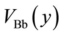 indicates the electric potential at the position y in the left side of the potential barrier.
 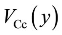 indicates the electric potential at the position y in the right side of the potential barrier. The values of
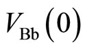 ,
, 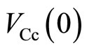 ,
,  and
and 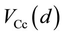 are nearly equal to the potentials at the probes B, C, b and c, respectively, as follows:
 (13)
(13)
where d is the width of the device as illustrated in Figure 9. The left panel of Figure 10 shows the case of 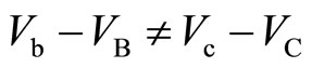 which is named Case I. The right panel shows the Case II where
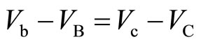 . In the Case I, the potential difference between both sides of the central barrier, namely,
  varies with the coordinate y as seen in the left panel of Figure 10. When
 , the potential difference
  is identical to
  for any position y as in the right panel of Figure 10. In this Case II, the frequency of the stimulated emission is the same for any position y.
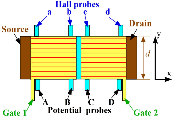
Figure 9. Top view of the tunneling device. There is a potential barrier in the central part (blue region) of the device. Horizontal red lines indicate the centres of y-direction for Landau orbitals with L = 0. The interval between the red lines is enlarged to bring them into view. The width of the device is described by the symbol d.
This means that the stimulated emission at any y-position is induced at the same frequency. The property produces the tunneling phenomenon like ac-Josephson effect. Consequently the following condition is required in the present experiment.
 (14)
(14)
That is to say the Hall voltage at the left area of the central barrier,  , is equal to that at the right area. Therefore the filling factor at the left area is the same as that at the right area. This condition can be satisfied by adjusting both voltages of the Gates 1 and 2.
(Condition 5)
If there are many impurities and lattice defects in the device, the coherent length becomes very short. Then the tunneling effect is disturbed by these impurities and lattice defects. Therefore it is necessary that the coherent length is longer than the width of the potential barrier. That is to say, the device is of good quality to ensure a sufficiently long coherent length.
(Condition 6)
The diagonal resistance in the FQH states must be sufficiently small for observing the tunneling effect. Figure 11 shows schematically a comparison between the di-
Case I: Case II:
Figure 10. Position-dependence of electric potential in both side of the potential barrier. Blue curve indicates the electric potential in the left side of the potential barrier; Skyblue and red curves indicate the electric potential in the right side of the potential barrier.
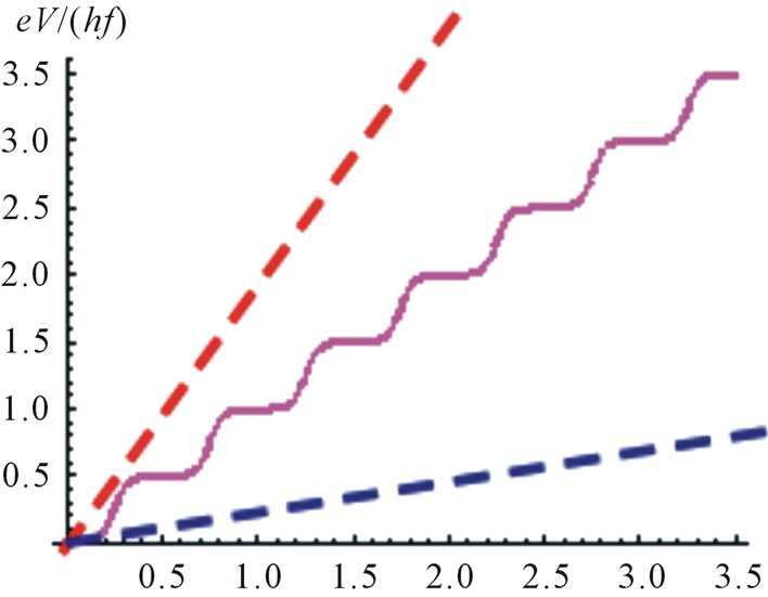
Figure 11. (I,V) curve of a new experiment. Red dashed line indicates Ohm’s law with the large diagonal resistance; Blue dashed line indicates Ohm’s law with the small diagonal resistance.
agonal resistance and the tunneling effect. If the device has a small diagonal resistance shown by blue dashed line, then we can observe the tunneling effect. On the other hand if the device has a large diagonal resistance shown by red dashed line, the tunneling effect will be masked by the large diagonal resistance. Accordingly the quantum Hall device must be fabricated so as to have an ultra high mobility.
(Condition 7)
The confinement of the Hall resistance in the FQHE becomes weak for an ultra small size of the device. Accordingly it is necessary to use an appropriate size of device with a large binding energy at the specific filling factor  and so on.
5. Short Summary
We have proposed the new experiment to observe the tunneling phenomenon between two quantum Hall states beyond the potential barrier. The seven conditions should be satisfied to observe the tunneling effect. If the stairlike curve is observed in the experimental  data, then it is confirmed that the phenomenon like the acJosephson effect certainly exists in the quantum Hall system. Furthermore the step value of the voltage determines the transfer charge in the tunneling effect. Thereby we can know which curve among the three curves of Figure 7 is realized in the 2D electron system.
6. Acknowledgements
The author expresses his heartfelt appreciation for support of Professor Masayuki Hagiwara. Also I wish to express appreciate for encouragement of Professor Koichi Katsumata, Professor Hidenobu Hori and Professor Yasuyuki Kitano. I cannot complete this article without their support.
REFERENCES
- K. V. Klitzing, G. Dorda and M. Pepper, Physical Review Letters, Vol. 11, 1980, pp. 494-497. doi:10.1103/PhysRevLett.45.494
- H. L. Stormer, “Nobel Lectures, Physics 1996-2000,” World Scientific, World Scientific Publishing Co. Pte. Ltd., pp. 295-325, 321.
- W. Pan, H. L. Stormer, D. C. Tsui, L. N. Pfeiffer, K. W. Baldwin and K. W. West, Physical Review Letters, Vol. 88, 2002, Article ID: 176802. doi:10.1103/PhysRevLett.88.176802
- S. Sasaki, e-Journal of Surface Science and Nanotechnology, Vol. 8, 2010, pp. 121-124. doi:10.1380/ejssnt.2010.121
- R. B. Laughlin, Physical Review B, Vol. 27, 1983, pp. 3383-3389.
- R. B. Laughlin, Physical Review Letters, Vol. 50, 1983, pp. 1395-1398. doi:10.1103/PhysRevLett.50.1395
- F. D. M. Haldane, Physical Review Letters, Vol. 51, 1983, pp. 605-608. doi:10.1103/PhysRevLett.51.605
- B. I. Halperin, Physical Review Letters, Vol. 52, 1984, pp. 1583-1586. doi:10.1103/PhysRevLett.52.1583
- S. M. Girvin, Physical Review B, Vol. 29, 1984, pp. 6012-6014. doi:10.1103/PhysRevB.29.6012
- S. C. Zhang, T. H. Hansson and S. Kivelson, Physical Review Letters, Vol. 62, 1989, p. 980. doi:10.1103/PhysRevLett.62.980.3
- J. K. Jain, Physical Review Letters, Vol. 63, 1989, pp. 199-202.
- J. K. Jain, Physical Review B, Vol. 41, 1990, pp. 7653- 7665. doi:10.1103/PhysRevB.41.7653
- R. K. Kamilla, X. G. Wu and J. K. Jain, Physical Review Letters, Vol. 76, 1996, pp. 1332-1335. doi:10.1103/PhysRevLett.76.1332
- B. Blok and X. G. Wen, Physical Review B, Vol. 42, 1990, pp. 8133-8144. doi:10.1103/PhysRevB.42.8133
- S. Sasaki, Advances in Condensed Matter Physics, Vol. 2012, 2012, Article ID: 281371. doi:10.1155/2012/281371
- S. Sasaki, Journal of Physics: Conference Series, Vol. 100, 2008, Article ID: 042022.
- S. Sasaki, “Binding Energies and Spin Polarizations of Fractional Quantum Hall States,” In: C. P. Norris, Ed., Surface Science: New Research, Nova Science Publishers, Hauppauge, 2006, pp. 103-161.
- S. Sasaki, Surface Science, Vol. 566, 2004, pp. 1040- 1046.
- S. Sasaki, Surface Science, Vol. 532, 2003, pp. 567-576.
- S. Sasaki, Proceedings of the 25th International Conference on the Physics of Semiconductors, Springer, New York, 2001, p. 925.
- S. Sasaki, Physica B, Vol. 281, 2000, pp. 838-839.
- E. Banghert, K. von Klitzing and G. Landwehr, Proceeding of the 12th International Conference on the Physics of Semiconductors, Stuttgart, 15-19 July 1974, p. 714.
- D. A. Broido and L. J. Sham, Physical Review B, Vol. 31, 1985, pp. 888-892.
- R. Wagner, “G-Factor, Effective Mass and Spin Susceptibility of a 2-Dimensional Electron Gas,” Master Thesis, University of Basel, Basel, 2009. http://zumbuhllab.unibas.ch/pdf/theses/masters/091209_Wagner_MScThesis_SdH.pdf