Journal of Modern Physics
Vol. 2 No. 8 (2011) , Article ID: 6674 , 9 pages DOI:10.4236/jmp.2011.28090
Control of Threshold and Gain of Parametric Amplification in Magnetoactive III-V Piezoelectric Semiconductors
1Department of Physics, Chaudhary Devi Lal University, Sirsa, India
2Department of Physics, Government Polytechnic for Women, Sirsa, India
E-mail: *vishu4up1181@gmail.com, prasut2003@yahoo.co.in
Received February 5, 2011; revised March 16, 2011; accepted April 17, 2011
Keywords: Parametric Gain, Piezoelectricity, Magnetostatic Field, Doped III-V Semiconductor
ABSTRACT
The effect of doping concentrations and a transverse external magnetostatic field on operational characteristics of parametric amplification of backward Stokes signal has been studied, using hydrodynamic model of semiconductors, in the far infrared regime. The model suggests three achievable resonance conditions: 1) lattice frequency and plasma frequency 2) stokes frequency and electron-cyclotron frequency 3) stokes frequency and hybrid (plasma and electron-cyclotron) frequency and these conditions have been utilised, on one hand, to substantially reduce the value of threshold intensity for onset of the parametric amplification and on the other hand, for switching of parametric large positive and negative gain coefficient (i.e. amplification and absorption). For example a strong transverse magnetostatic field 10.0 T with free carrier concentration 1.5 × 10¹⁹m–3 enhances the gain by a factor of 103 as in its absence. Results also suggest that a weakly piezoelectric III–V semiconductor duly illuminated by slightly off-resonant not-too-high-power pulsed lasers with pulse duration sufficiently larger than the acoustic phonon lifetime is one of promising hosts for parametric amplifier/frequency converter.
1. Introduction
The area of parametric interactions and their devices such as optical parametric amplifiers and oscillators (OPA/ OPO) occupies a special place in nonlinear optics due to their potential applications. Optical parametric amplifiers and oscillators are being extensively used in fabrication of tunable coherent radiation source with considerably high gain and high conversion efficiency [1]. Parametric interactions are also employed successfully to study the photon amplifiers [2,3] and to generate high peak power subpicosecond optical pulse [4]. The choice of a nonlinear medium and operating wavelength are crucial aspects in design and fabrication of parametric amplifiers and oscillators. Amongst different types of nonlinear media, semiconductors offer considerable flexibility for fabrication of optoelectronic devices because: 1) the large number of free electrons/holes available as majority charge carriers in doped semiconductors manifests many more exciting nonlinear optical processes [5]; 2) carrier relaxation times can be altered through design of materials and device structures; 3) large optical nonlinearities in the vicinity of band gap resonant transitions [6,7]; 4) either change in absorption or refractive index can be utilized; 5) devices may operate either at normal incidence or in waveguides; 6) devices are integrable with other optoelectronic components, 7) substantially transparent for photon energies less than the band gap energies [8]. Here it is worth mentioning that resonant and non-resonant optical nonlinearity of semiconductors have been utilised for fabrication of nonlinear optical devices. The resonant nonlinearities are large in magnitude [9], while, the magnitude of non-resonant optical nonlinearity (SNON) is small but its response time is fast due to virtual transition mechanisms. In order to design and develop efficient parametric amplifiers/oscillators, different types of nonlinear materials have been used [10,11]. However, recent trend reveals that still there is a great need to explore alternatives, particularly those compatible with semiconductor technology, due to the rapid growth of planar devices such as wavelength division multiplexers and add-drop filters in advanced networks. A hybridly integrated semiconductor optical amplifier Mach–Zehnder interferometer (MZI) was demonstrated using bidirectional data injection and an additional external continuous wave signal for differentially biasing the interferometer arms, optimizing gain and phase conditions during the switching functionality [12]. A long period linear grating is imprinted on semiconductor waveguide and using second-order susceptibility its frequency converters of high frequency is experimentally demonstrated [13].
It is well known that the manipulation of threshold condition and gain are important issues to improve the efficiency and functionality of parametric devices (e.g. amplifiers, oscillators and frequency converters). In case of semiconductors, doping (free carriers), composition and micro-structuring have been mostly exploited for improving the performance of optoelectronic devices [14, 15]. Besides, optical nonlinearities of semiconductors can be easily modified by externally applied electric and magnetic fields and hence external field dependent property has been exploited to understand the mechanisms involved in nonlinear processes such as electro-optic and magneto-optic effects and fabrication of devises based on it [16,17]. Makowska et. al. [18] pointed out that optical second harmonic generation (SHG) can be induced in both single and polycrystalline InAs by acoustic wave and found that efficiency of SHG depends on acoustic power. However, in case of layered periodic structure of III-V semiconductor-plasma, a significant increase in efficiency of nonlinear interaction is obtained near the nonlinear resonances [19]. Voigt geometrical configuration has been used to enhance the terahertz emission and the photo-refraction in III–V semiconductors [16,17]. Of-late authors have made systematic attempt to explore the influence of free carrier concentration, externally applied magnetostatic field and excitation intensity on second order susceptibility of weakly piezoelectric n-type III–V semiconductors [20]. In the present article, the model [20] has been further extended to study operational characteristic of parametric amplification and explore the possibility of switching of optical nonlinearity by applied magnetostatic field. Using the coupled-mode theory, expression for operational characteristic parameters of parametric amplifiers (i.e. threshold condition, parametric gain) has been derived. Finally, exhaustive numerical analysis is performed with a set of data appropriate for weakly piezoelectric semiconductor-plasma (n-InSb) duly irradiated by a 10.6 µm CO2 laser to establish the application of the present model. The results indicate that the threshold condition and parametric gain can be manipulated by varying doping concentration, magnetostatic field and excitation intensity.
2. Theoretical Formulations
In the present section, expression of threshold condition for the onset of backward coherent scattered stokes wave and its gain coefficient are obtained, in weakly piezoelectric doped III-V semiconductors, under off-resonant transition regime in the absence and the presence of external applied magnetostatic field.
In doing so we assume the pump wave (laser) energy ( ) < band gap energy (
 ) of semiconductor. The pulse duration of laser is much larger than the material damping time such that the interaction is treated to be of a steady-state type. Further we consider that there are many photons in the pump wave and it can be described by plane wave. The scheme of three-wave mixing (pump wave, backward scattered stokes wave and acoustic signal wave) mechanism within matter in the presence of an external magnetostatic field is shown in Figure 1. We assume the pump electric field
is polarised along z-axis and incident on ( ) surface of the crystal. Let us assume the electric field of pump radiation produces longitudinal acoustic wave (i.e. idler wave),
 and in turn it scatters the pump wave. We further assume that the backward scattered stokes wave, say
 is also polarised along z-axis. In order to study parametric amplification in Voigt geometry an external transverse magnetostatic field (B0) is applied parallel to z-axis.
The momentum and energy transfer between these waves can be described by phase matching conditions:  and
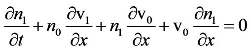
and , where the frequencies {ωp, ωs, ωa} and wave vectors {kp, ks, ka} correspond to the incident laser, the backward scattered Stokes wave and the acoustic wave, respectively. We also consider hydrodynamic model of the homogeneous one component (viz., n-type) semiconductor, satisfying the condition
  (
( and
and  being the acoustic wave number and the electron mean free path, respectively). This condition implies that the sound wavelength is much greater than the mean free path of electrons, so that the motion of the carriers under the influence of the external field is averaged out. In addition, it allows neglecting the non-uniformity of the high frequency electric field under the dipole approximation [21].
The zeroth-order electron momentum transfer equation under the influence of magnetostatic field can be de-
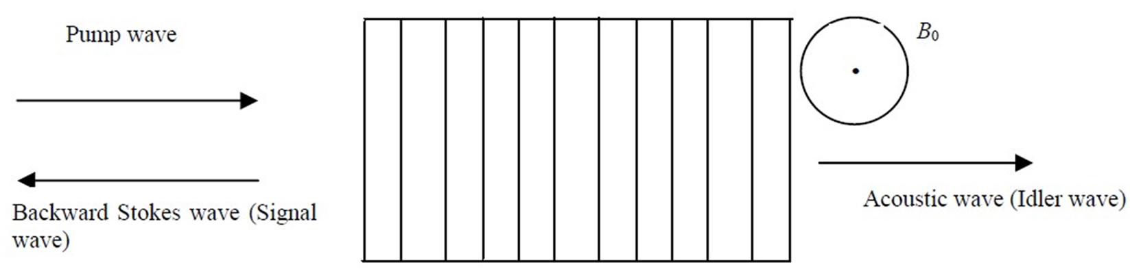
Figure 1. Schematic diagram for interaction of pump wave with doped III-V piezoelectric semiconducting crystal in the presence of magnetostatic field.
scribed as
 (1)
(1)
where .
.
The first-order electron momentum transfer and continuity equation in the presence of external magnetostatic field are defined [20] by
 . (2)
. (2)
 (3)
(3)
where  and
and  are zerothand first-order oscillatory fluid velocities of the electron of effective mass m and charge –e.
  and
and  are initial and perturbed electron density and
  is the electron collision frequency. It is a well-known fact that the effective mass of an electron in III–V semiconductors is smaller than the effective mass of a hole and therefore the drift velocity of a hole is less than the drift velocity of an electron and hence the effect of hole on nonlinearity can be neglected.
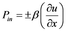
The pump wave produces stress in the medium and the linear relationship between stress and electric field is described by piezoelectricity. The origin of piezoelectricity lies in the first order force ( , where β
is piezoelectric coefficient). In particular, in narrow bandgap weakly piezoelectric III-V semiconductors such as InSb and InAs, the high mobility of electrons (due to their low effective mass) allows one to work at drift velocities several times the sound velocity and thus keep the effects of inhomogeneities to a minimum [22].
Let us consider, if the deviation of lattice along x-direction is u(x, t), due to stress in the medium, in the presence of an external magnetostatic field then the strain can be described as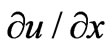 and the resultant polarisation (Pin) can be given as
 (4)
(4)
Taking into account the effect of piezoelectricity, the modified equation of motion of lattice vibrations may be defined as
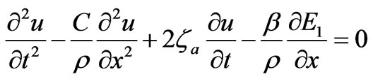 . (5)
. (5)
where ,
,  and
and  being the mass density, material’s elastic constant, acoustic phonon damping parameter and E1 is being space charge electric field of the medium which can be obtained from Poisson’s equation as
 . (6)
. (6)
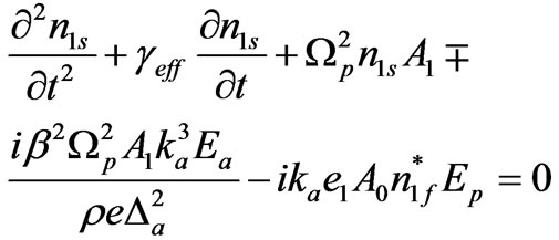
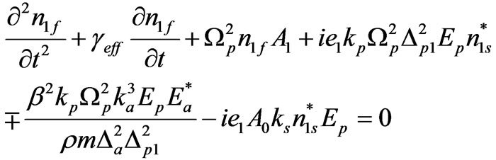
Now we are interested to derive expression for firstorder perturbed carrier-density of piezoelectric doped semiconductors due to three-wave mixing. Under rotating wave approximation and using Equations (1)-(6) a simplified expression for the density perturbation is obtained as
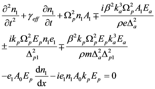 (7)
(7)
where  (electron-plasma frequency),
  (electron-cyclotron frequency),
  ,
,
 ,
,  ,
,
 ,
,  ,
,
and .
.
In obtaining Equation (7) we have neglected the Doppler shift under the assumption that  (
( being the velocity of an acoustic wave) and higher order terms like
 . Equation (7) states that density perturbation may oscillates at low (acoustic, ωa) and high (stokes, ωs) wave frequency components and that can be expressed as:
 . The higher-order terms with frequencies
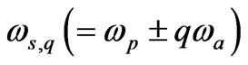 , for
, for  will be off-resonant and are neglected in the study of second-order nonlinearities in doped semiconductors. Using phase matching conditions, low and high frequency density perturbation can be obtained from Equation (7) as
 (8)
(8)
and
 (9)
(9)
By solving coupled Equations (8) and (9), expression of  (low frequency component) and
  (high frequency component) can be obtained as well as their values may be computed by using material parameters and electric field amplitudes in the absence and presence of transversely applied magnetostatic field. The expression of
  is obtained as
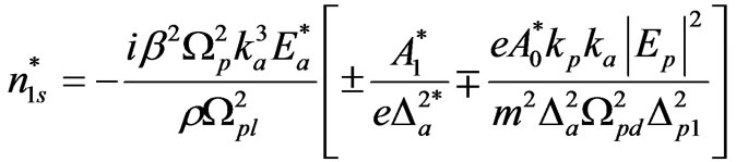 (10)
(10)
where
 and
and 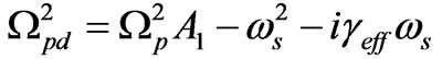 .
.
By knowledge of the first-order carrier density perturbation, second-order polarisation at backward Stoke’s frequency can be obtained by time integral of induced current density 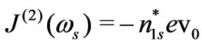 as
as
 . (11)
Using Equations (10) and (11), effective second-order optical complex susceptibility is obtained as
 (12)
(12)
where
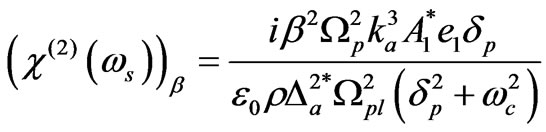 (12a)
(12a)
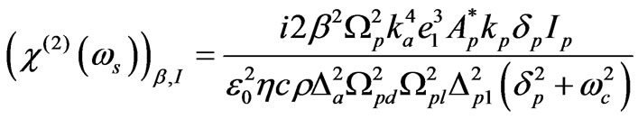 (12b)
(12b)
with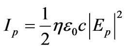 .
.
Using algebra, expression for real and imaginary parts of (12a) and (12b) can be obtained. It is well known fact that real and imaginary part of optical susceptibility describes refraction and gain/absorption phenomena in the crystal, respectively. By knowledge of propagation of light in refractive medium various optical devices have been designed and fabricated such as optical wave guide, filters, amplifiers, oscillators, coupler etc [11,17].
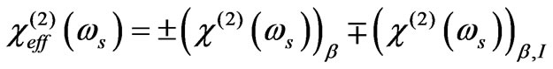
The present article is focused to study behavior of the threshold condition for parametric amplification and gain coefficient ( ) of backward coherent scattered stoke mode by varying free carrier density and externally applied magnetostatic field. In doing so, well known following expression [1] is used
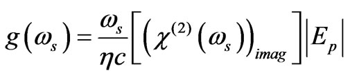 (13)
(13)
3. Results and Discussion
In order to explore the applicability of the model, a detailed numerical study of threshold condition and gain behavior of parametric amplification has been made. Efforts are also made to find out conditions for achieving large gain with low power laser. In doing so, we consider the irradiation of n-type doped III-V micro size semiconductor sample (such as InSb) by 10.6 µm CO2 at liquid nitrogen temperature (77 K). Around this temperature, absorption coefficient of the sample is low around 10 μm and one may neglect contribution due to bandto-band transition mechanism. It is worth pointing that at 77 K temperature, the dominant mechanism for transfer of momentum and energy of the electron in scattered mode is due to the acoustic phonon scattering in semiconductors [23,24].
The following material parameters are taken as representative values to establish the theoretical formulation:
ωp = 1.78 × 10¹⁴ s−1, ωa = 2 × 10¹¹ s−1, ωs = 1.77 × 10¹⁴ s−1, m = 0.014m0 (m0 being the rest mass of an electron), εl = 15.8, ρ = 5.8 × 10³ kgm−3, η = 3.8, β = 0.054 cm−2, γ = 3 × 10¹¹ s−1, va = 4 × 10³ ms−1, ka= 5 × 10⁷ m–1,  = 2 × 10¹⁰ s–1, c = 3 × 10⁸ ms–1
3.1. Threshold Condition
The threshold pump intensity (Ipth) required for the onset of parametric amplification is obtained by setting imaginary part of Equation (12) equals to zero. Ipth, obtained
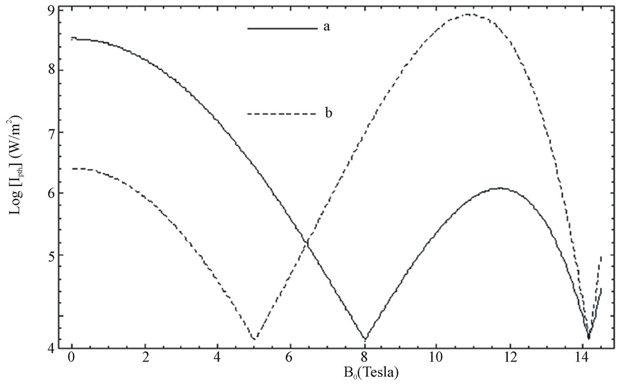
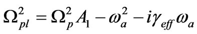
Figure 2.1. Variation of threshold pump intensity (Log [Ipth]), for Equation (12a), with magnetostatic field (B0) at free carrier concentration (a) n0 = 1.5 × 10¹⁹ m–3 and (b) n0 = 2.4 × 10¹⁹ m–3.
from Equation (12a), versus with an external magnetostatic field for two different free carrier concentrations i.e. (a) n0 =1.5 × 10¹⁹ m–3 and (b) n0 = 2.4 × 10¹⁹ m–3 is plotted in Figure 2.1. One may notice that in the absence of magnetostatic field, a large Ipth is required for onset of parametric amplification. For example, when B0 = 0.0 T, we found Ipth ~ 3.7 × 10⁸ Wm−2 and 3.0 × 10⁶ Wm−2 for n0 = 1.5 × 10¹⁹ m–3 and 2.4 × 10¹⁹ m–3, respectively.
When B0 > 0, Ipth reduces considerably due to resonance conditions. Let us focus on the threshold condition for parametric amplification when piezoelectricity is solely responsible for parametric interaction. In this case, minimum threshold intensity can be achieved in two different range of externally applied magnetostatic field, i.e. 1) moderate and 2) strong magnetostatic fields. In former case, a minimum value of threshold intensity is found ~1.1 × 10³ Wm−2 (for B0 = 5.0 T, n0 = 2.4 × 10¹⁹ m−3). The minima of threshold intensity arises due to resonance condition; . It is also noticed that the position of minima shifts toward lower magnetostatic field with increasing doping concentration. While in later case, Ipth can be achieved when
 . For example, when B0 = 14.1 T, Ipth
~1.2 × 10³ Wm−2. Here it is worth pointing out that in later case a small change in free carrier concentration does not affect shifting position of minima. This result is well in agreement with the result of Palik and Furdyna [25].
In order to study the role of different physical mechanism leading to parametric interaction we have used Equation (12b) to obtain threshold condition for onset of parametric amplification due to coupling between the piezoelectric coefficient and pump electric field. The threshold pump intensity, determined from Equation (12b), versus external magnetostatic field for two different samples having free carrier concentration i.e. (a) n0 = 1.5 × 10¹⁹ m–3 and (b) n0 = 2.4 × 10¹⁹ m–3, is plotted in Figure 2.2. One may observe that when B0 = 0.0 T, Ipth required for onset of parametric amplification is 5.9 × 10⁶ Wm−2. The figure depicts that the minima of Ipth is independent of change of free carrier concentration. The model suggests that when B0 > 0, a minimum Ipth can be achieved at three different values of magnetostatic field due to three different resonance conditions:
 ,
, 
and . Around the first resonance condition, the minimum Ipth is found to be 3.0 × 10⁴ Wm−2. This resonance condition also shifts the position of minima towards lower magnetostatic field with increase in free carrier concentration. However, the second and the third resonance conditions yield Ipth ~ 1.1 × 10³ Wm−2 and 1.9 × 10⁶ Wm−2, respectively. It is noticed that around the second and third resonance conditions the position of minima are nearly independent with the variation of doping concentrations. A comparison of the results obtained from Equation (12a) and (12b) reveal that the required minimum Ipth for the onset of parametric amplification due to parametric coupling of piezoelectric coefficient and pump electric field is nearly 100 times higher than the value obtained due to solely piezoelectricity. In the forthcoming analysis to study the behavior of parametric gain we consider Ip = 1.5 × 10¹¹ Wm−2 as a representative excitation intensity which is well above the threshold intensity but below the damage threshold of the sample [26].
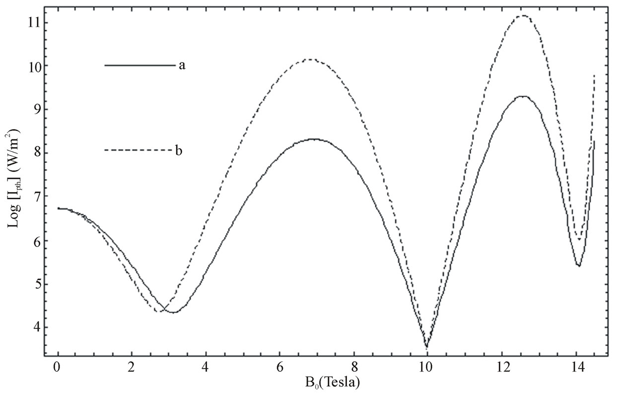
Figure 2.2. Variation of threshold pump intensity (Log[Ipth]), for Equation (12b), with magnetostatic field (B0) at free carrier concentration (a) n0 = 1.5 × 10¹⁹ m–3 and (b) n0 =2.4 × 10¹⁹ m–3.
3.2. Parametric Gain
The Equation (13) with (12) shows the dependence of parametric gain on controllable physical parameters namely free carrier concentration (through plasma frequency, Ωp), external applied magnetostatic field (through cyclotron frequency, ωc) and pump Intensity (Ip).
Figure 3.1 shows the behavior of parametric gain at stokes frequency ( ), obtained using Equation (13) with Equation (12a), by varying B0 and n0 simultaneously. The figure clearly shows substantial enhancement of
  and change in its sign. This typical behavior arises due to resonance condition:
(resonance between scattered stokes wave frequency and modified electron-cyclotron wave frequency). At the resonance condition, magnetostatic field dependent drift velocity becomes many times larger than the acoustic wave velocity and due to which interaction between plasmon and acoustic phonon becomes strong. The resonance condition allows one to select typical value of B0 and n0 at which maximum gain can be achieved. A small change in typical value of B0 and n0 leads to decrease in the value of positive gain coefficient and further change gives rise to maximum negative gain (i.e. maximum absorption).
By selecting appropriate value of B0 (say 9.0 T) and n0 (say 1.5 × 10¹⁹ m–3), we obtained  ~ 396 m–1. By varying B0 and n0 simultaneously, the change in sign of
  can also be observed. Besides, it is noticed that when the sample is subjected to moderate magnetostatic field, i.e. 0.0 < B0 < 10.5 T, the value of
  varies almost parabolically with rising n0. The theoretical model also suggests possibilities of shifting in frequency of coherent backward stokes modes towards higher value of B0 (i.e. blue shift) as plasma frequency (through n0) approaches twice of acoustic wave frequency. After departure from the resonance condition, the parametric gain becomes negative (absorption) and saturates to very small value. However, in the absence of external magnetostatic field (B0 = 0) and n0 = 1.5 × 10¹⁹ m–3, the value of
  is 7.4 m–1 which is nearly 50 times smaller than the value obtained around the resonance condition.
The salient feature of result is the switching of positive and negative gain between high value to low value by varying independently/simultaneously B0 and n0 and also achieving its large value in III-V weakly piezoelectric semiconductors. The result suggests the possibility of devise of parametric switches in far infrared region.
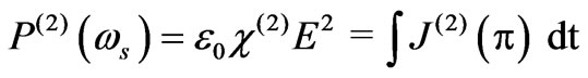
Figure 3.2 shows variation of the gain coefficient , using Equation (12b), with respect to B0 and n0. This figure also depicts the enhancement of
  as well as change in its sign. In this case, enhancement and switching of the gain occurs due to resonance conditions: 1)
  and 2)
 . Interesting feature of this case is the interaction between plasmon oscillator and electron-cyclotron oscillator in the presence of excitation intensity. It is often advantageous, moving the frequency of coherent stokes wave to higher and more accessible spectral region in proportion to: a) plasma frequency (or n0) for fixed electroncyclotron frequency (or B0), b) electron-cyclotron frequency for fixed plasma frequency and c) combination of both frequencies. For example, in moderately doped semconconductor (n0 = 1.5 × 10¹⁹ m–3), low externally applied
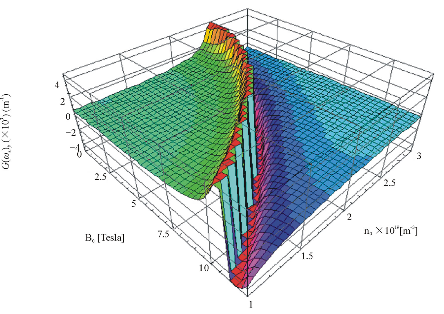
Figure 3.1. Variation of  with magnetostatic field (B0) and free carrier concentration (n0).
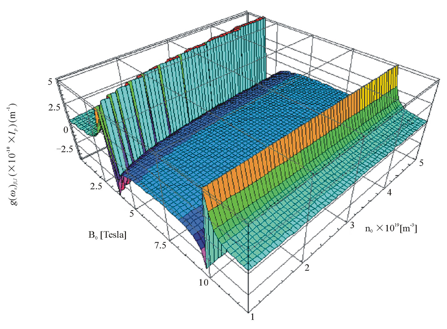
Figure 3.2. Variation of  with magnetostatic field (B0) and free carrier concentration (n0).
magnetostatic field (1.5 - 3.0 T) yields a large value of  and also alters its sign as well as shifts the stokes frequency towards higher frequency (Blue shift). With further increase in B0, the second resonance condition (
 ) yields sharp enhancement and change of sign of
  at B0 = 10.0 T.
In addition to the B0 and n0 dependence, the parametric gain can also be enhanced by increasing the value of excitation intensity. Here it is worth mentioning that practically the excitation intensity can not be increased arbitrarily because it may optically damage the sample [26].
4. Conclusions
In the present study, using electromagnetic treatment the operational characteristic of the parametric amplifier has been studied in weakly piezoelectric narrow direct-gap III–V doped semiconductors like n-InSb subjected to a transverse magnetostatic field under off-resonant transition regime. The following important conclusions may be drawn:
1) The hydrodynamic model of semiconductor-plasma has been successfully applied to study the effect of doping level, transverse magnetostatic field and pump intensity on operational characteristic of parametric amplifiers (i.e. threshold condition and optical parametric gain/ absorption) in piezoelectric III–V doped semiconducting crystals duly illuminated by slightly off-resonant not-toohigh-power pulsed lasers with pulse duration sufficiently larger than the acoustic phonon lifetime.
2) Resonance conditions between 1) lattice frequency and plasma frequency 2) stokes frequency and electron-cyclotron frequency 3) stokes frequency and hybrid (plasma and electron-cyclotron) frequency may be utilized, on one hand, to reduce the threshold intensity for onset of parametric amplification. On the other hand, switching of parametric gain between the low and high value and hence open up the possibility of devising optical switch. A strong transverse magnetostatic field (10.0 T) enhances the gain by a factor of 103 as in its absence.
3) The technological potentiality of a magnetoactive III-V semiconductor-plasma as the host for parametric devices like parametric amplifiers and oscillators are established. In III-V crystals, parametric amplification and oscillation in the infrared regime appears quite promising under the resonance conditions and replaces the conventional idea of using high power pulsed lasers.
5. Acknowledgements
One of the authors (PA) acknowledges financial support from Department of Science and Technology (FIST), New Delhi, India. Dr. K.C. Bhardwaj (Vice-chancellor) is also acknowledged for his constant encouragement.
REFERENCES
- R. L. Bayer, “Nonlinear Optics,” Academic Press, London, 1975, pp. 47-159.
- C. K. Hong and L. Mandel, “Theory of Parametric Frequency down Conversion of Light,” Physical Review A, Vol. 31, No. 4, 1985, pp. 2409-2418. doi: 10.1103/PhysRevA.31.2409
- Z. Y. Ou, L. J. Wang and L. Mandel, “Photon Amplification by Parametric Down Conversion,” Journal Optical Society America, Vol. B7, 1990, pp. 211-214.
- J. Zyss, I. Leodoun, J. Badan, J. L. Oudar, J. Etchepare, D. Hulin, A. Mingus and A. Antonnetii, “Amplification at Emission Paramétriques à l'Échelle Subpicoseconde dans un Crystal Organique: Application à la Spectroscopy InfraRouge,” Revue de Physique Appliquée, Vol. 22, No. 10, 1987, pp. 1229-1238.
- D. A. B. Miller, “Bistable Optical Devices: Physics and Operating Characteristics of Nonlinear Optics in Semiconductors,” Laser Focus, Vol. 19, 1983, pp. 61-68.
- R. K. Jain, “Degenerate Four-Wave Mixing in Semiconductors: Application to Phase Conjugation and to Picoseconds Resolved Studies of Transient Carrier Dynamics,” Optics Engineering Bellingham, Vol. 21, 1982, pp. 199-218.
- S. D. Smith, “Lasers: Nonlinear Optics and Optical Computers,” Nature, Vol. 316, 1982, pp. 319-324. doi: 10.1038/316319a0
- P. A. Wolff, “Nonlinear Optics,” Academic Press, London, 1977, pp. 169-212.
- E. Garmire, “Resonant Optical Nonlinearities in Semiconductors,” IEEE Journal Quantum Electronics, Vol. 6, No. 6, 2000, pp. 1094-1110. doi: 10.1109/2944.902158
- R. W. Boyd, “Nonlinear Optics,” Academic Press, San Diego, 1992, Ch. 9, pp. 409-450.
- M. J. Connelly, “Semiconductor Optical Amplifiers,” Springer-Verlag, Boston, 2002.
- D. Apostolopoulos, K. Vyrsokinos, P. Zakynthinos, N. Pleros and H. Avramopoulos, “An SOA-MZI NRZ Wavelength Conversion Scheme with Enhanced 2R Regeneration Characteristics,” IEEE Photonics Technology Letter, Vol. 21, No. 19, 2009, pp. 1363-1365. doi. 10.1109/LPT.2009.2026725
- A. Hayat, Y. Elor, E. Small and M. Orenstein, “Phasematching in Semiconductor Nonlinear Optics by Linear Long-Period Gratings,” Applied Physics Letter, Vol. 92, No. 18, 2008, pp. 181110-112. doi: 10.1063/1.2918013
- G. Lutz, “Semiconductor Radiation Detectors: Device Physics,” Springer, Berlin, 1999.
- Y. Fu and M. Willander, “Physics Models of Semiconductor Quantum Devices,” Springer, Berlin, 1999. doi: 10.1007/978-1-4615-5141-6
- M. B. Johnston, D. M. Whittaker, A. Dowd, A. G. Davies, E. H. Linfield, X. Li and D. A. Ritchie, “Generation of High-Power Terahertz Pulses in a Prism,” Optics Letters, Vol. 27, No. 21, 2002, pp. 1935-1937. doi: 10.1364/OL.27.001935
- G. Meinert, L. Banyai, P. Gartner and H. Haug, “Theory of THz Emission from Optically Excited Semiconductors in Crossed Electric and Magnetic Fields”, Physical Review B, Vol. 62, 2000, pp. 5003-5009. doi: 10.1103/PhysRevB.62.5003
- J. M. Makowska, K. J. Plucinski, A. Hruban, J. Ebothe, J. I. Fuks and I. V. Kityk, “Acoustically Induced Optical Second Harmonic Generation in InAs,” Semiconductor Science & Technology, Vol. 19, No. 11, 2004, pp. 1285- 1290. doi: 10.1088/0268-1242/19/11/013
- A. A. Bulgakov and O. V. Sharmkova, “Nonlinear Interaction of Waves in Semiconductor Plasma,” Journal Physics D: Applied Physics, Vol. 40, No. 9, 2007, pp. 5896- 5901.doi: 10.1088/0022-3727/40/19/017
- B. Lal, P. Aghamkar, S. Kumar and M. K. Kashyap, “Second-Order Optical Susceptibility in Doped III-V Piezoelectric Semiconductors in the Presence of a Magnetostatic Field,” European Physics Journal D, Vol. 61, No. 3, 2011, pp. 717-724. doi: 10.1140/epjd/e2010-10455-9
- P. K. Kaw, “Parametric Excitation of Ultrasonic Waves In Piezoelectric Semiconductors,” Journal Applied Physics, Vol. 44, No. 4, 1973, pp. 1497-1498. doi: 10.1063/1.1662399
- D. L. Spears, “Brillouin Scattering Study of Propagating Acoustoelectric Domains in n-GaAs,” Physical Review B, Vol. 2, No. 6, 1970, pp. 1931-1951. doi: 10.1103/PhysRevB.2.1931
- D. L. Rode, “Semiconductors and Semimetals,” Academic, New York, 1975, Ch. 1, pp. 5-17.
- G. E. Stillman, C. M. Wolfe and J. O. Dimmock, “Hall Coefficient Factor for Polar Mode Scattering in n-Type GaAs,” Journal Phys Chem Solids, Vol. 31, No. 6, 1970, pp. 1199-1204. doi: 10.1016/0022-3697(70)90122-8
- E. D. Palik and J. K. Furdyna, “Infrared and Microwave Magnetoplasma Effects in Semiconductors,” Report Progress in Physics, Vol. 33, No. 3, 1970, pp. 1193-1322. doi: 10.1088/0034-4885/33/3/307
- J. M. Mayer, F. J. Bartoli and M. R. Kruer, “Optical heating in Semiconductors,” Physical Review B, Vol. 21, No. 4, 1980, pp. 1559-1568. doi: 10.1103/PhysRevB.21.1559