Wireless Engineering and Technology
Vol.3 No.4(2012), Article ID:24177,4 pages DOI:10.4236/wet.2012.34027
A Brief Review: Stage-Convertible Power Amplifier Using Differential Line Inductor
![]()
School of Electronic Engineering, Soongsil University, Seoul, Korea.
Email: pck77@ssu.ac.kr
Received September 6th, 2012; revised October 4th, 2012; accepted October 15th, 2012
Keywords: Inductor; Differential Line Inductor; Matching Network; Power Amplifier; Stage-Convertible
ABSTRACT
In this review article, a stage-convertible RF power amplifier designed with a 0.18-mm RF CMOS process is described. A method to implement a low-power matching network is an essential technology for the stage-convertible power amplifier. Various low-power matching networks with distributed active transformers as an output power combiner are compared in terms of the amounts of undesired coupling, the chip size, and the amount of power loss. The feasibility of a differential line inductor for the stage-convertible power amplifier is assessed and explained. Finally, we show that the differential line inductor is a realistic means of reducing the overall chip size, enhancing the quality factor of the matching network, and minimizing the undesired coupling between the inter-stage matching network and any output matching network. Additionally, the operating mechanism of the stage-convertible power amplifier using the differential line inductor for a low-power matching network is described in detail.
1. Introduction
Recently, the multi-mode RF CMOS power amplifier has been studied vigorously in an effort to extend battery lifetimes [1-3]. Given that, statistically, the power transmitted in a wireless system is below the maximum for most of the transmission time, the average power efficiency is far below its maximum. It is, therefore, essential to maintain a high level of efficiency over a wide range of output power when seeking to enhance the average power efficiency [4-8].
Various stage-convertible power amplifiers have been introduced in an effort to improve the efficiency of these devices when used in a low-output-power region. Interstage matching networks for a stage-convertible power amplifier require inductance to achieve high load impedance in the low-power mode. The required level of inductance can be designed using a line inductor, a transmission line transformer, or a spiral-type inductor. However, because the inductance of a line inductor is relatively low compared to that of a spiral-type inductor, line inductors are not suitable for GHz-order amplifier applications. On the other hand, although the spiral-type inductor has sufficient inductance for GHz-order amplifier applications, their bulky size becomes an obstacle which prevents a compact layout [9]. Additionally, undesirable coupling may occur between the spiral-type inductor and the output matching network, which can degrade the overall performance of the amplifier due to the bulky size of the spiral-type inductor.
In this review article, a differential line inductor intended to solve the problems arising from the low inductance of the line inductor and the bulky size of the spiraltype inductor is used in conjunction with the inter-stage matching of a stage-convertible power amplifier [9]. The differential line inductor is shown to be suitable for use with a differential RF circuit. We demonstrate that the differential line inductor can resolve the size and desired inductance issues of the stage-convertible power amplifier.
2. Conventional Stage-Convertible Power Amplifier
Figure 1 shows a simplified block diagram of a conventional stage-convertible power amplifier. The power generated at the driver stage drives the power stage and transfers the load of the amplifier through the low-power matching network. The load impedance of the driver stage needs to be higher than that of the power stage for high efficiency in the low-output-power region. The matching network at “Path 1” shown in Figure 1 creates RLOAD2 high impedance as compared to RLOAD1 [8].
Generally, the matching network at “Path 1” is composed of the series inductance and shunt capacitance. Figure 2 shows the contour of the load impedance trans-
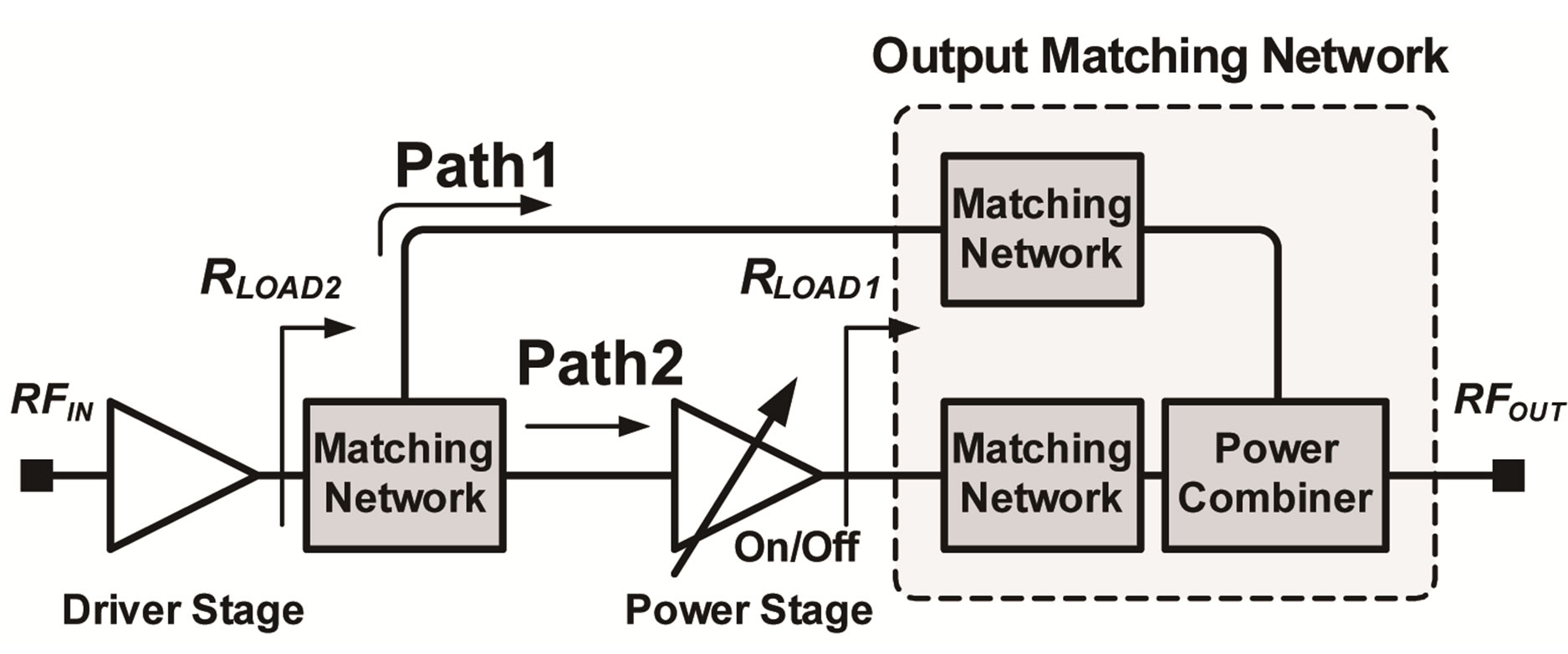
Figure 1. Block diagram of a stage-convertible power amplifier.
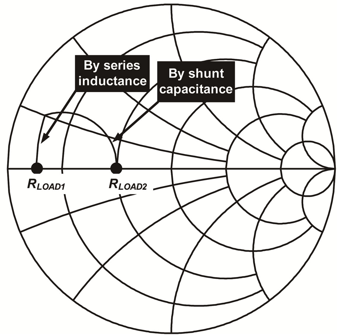
Figure 2. Contour of the transformation of the load impedance at a stage-convertible amplifier.
formation mechanism at the stage-convertible amplifier. The load impedance RLOAD1 of the power stage is transformed to RLOAD2 of the driver stage by means of the series inductance and shunt capacitance. Thus, the load impedance RLOAD2 becomes higher than RLOAD1.
The stage-convertible power amplifier generally has two modes: the high-power mode and the low-power mode.
1) High-Power Mode: All of the stages are turned on. Most of the output power of the amplifier is generated by the power stage of the amplifier. The load impedance of the power stage, RLOAD1, should be designed as low enough to obtain watt-level output power.
2) Low-Power Mode: For the low-power mode, the power stage is turned off. Most of the output power of the amplifier is generated by the driver stage of the amplifier because the output node of the driver stage is connected to the power amplifier output node through the low-power matching network. The load impedance of the driver stage, RLOAD2, should be higher than RLOAD1 to ensure high efficiency in the low-output-power region.
One of the most simple low-power matching networks for a stage-convertible power amplifier is shown in Figures 3 and 4. The shunt capacitor includes the parasitic capacitances of the drain-source capacitance of the driver stage and the gate-source capacitance of the power stage, as well as an additional MIM capacitor. The series inductance levels can be designed using a spiral-type inductor and line inductor, as shown in Figures 3 and 4,

Figure 3. Block diagram of a stage-convertible power amplifier using a conventional spiral inductor.
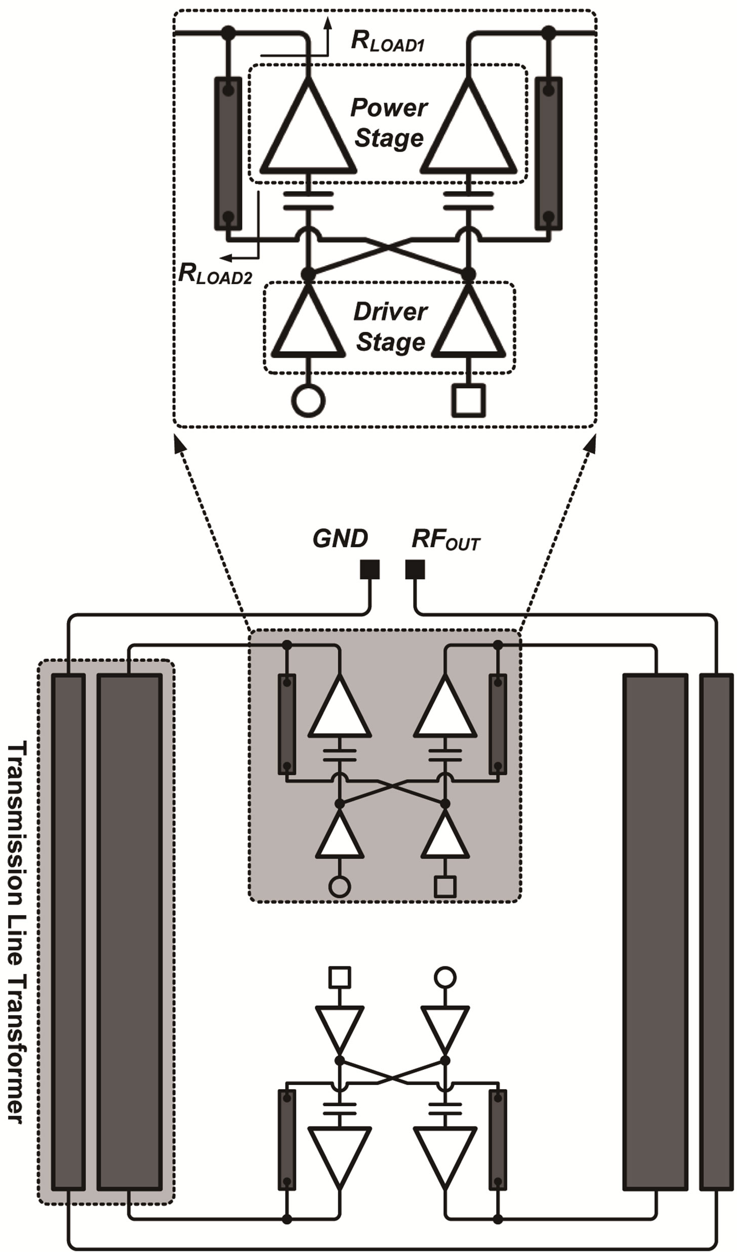
Figure 4. Block diagram of a stage-convertible power amplifier using a conventional line inductor.
respectively. A DC-blocking capacitor between the driver stage output and the power stage input is needed due to the different biases between the power stage input and the driver stage output.
In Figure 3, the spiral inductor is used as one of the low-power matching components. However, inserting the spiral inductor inside the distributed active transformer generates several problems due to the bulky size of the spiral-type inductor. If the amplifier has two differential pairs of power and driver stages, four conventional spiral inductors are needed for the low-power matching network. In such a case, the space required by the four spiral inductors becomes very large and the length of the transmission line transformers for the distributed active transformer should be increased to ensure space for the inductors. The increased size of the distributed active transformer makes it difficult to obtain an optimum level of impedance from the output matching network and thus degrades the maximum output power and efficiency.
Additionally, the magnetic interaction between the low-power matching network and the output transformer leads to issues with the stability, the gain reduction, and the second harmonic. The lossy spiral inductor is such that the efficiency in the low-output-power region cannot be improved.
The use of a line inductor presents a possible solution in a low-power matching network for a stage-convertible power amplifier using a distributed active transformer, as shown in Figure 4. As described in the previous sections, the line inductor has a high quality factor and a compact size compared to a conventional spiral inductor. However, the inductance of the line inductor is insufficient for a low-power matching networks. Thus, the circuit architecture shown in Figures 3 and 4 must be modified for a high-performance stage-convertible power amplifier.
3. Proposed Power Amplifier Using the Differential Line Inductor
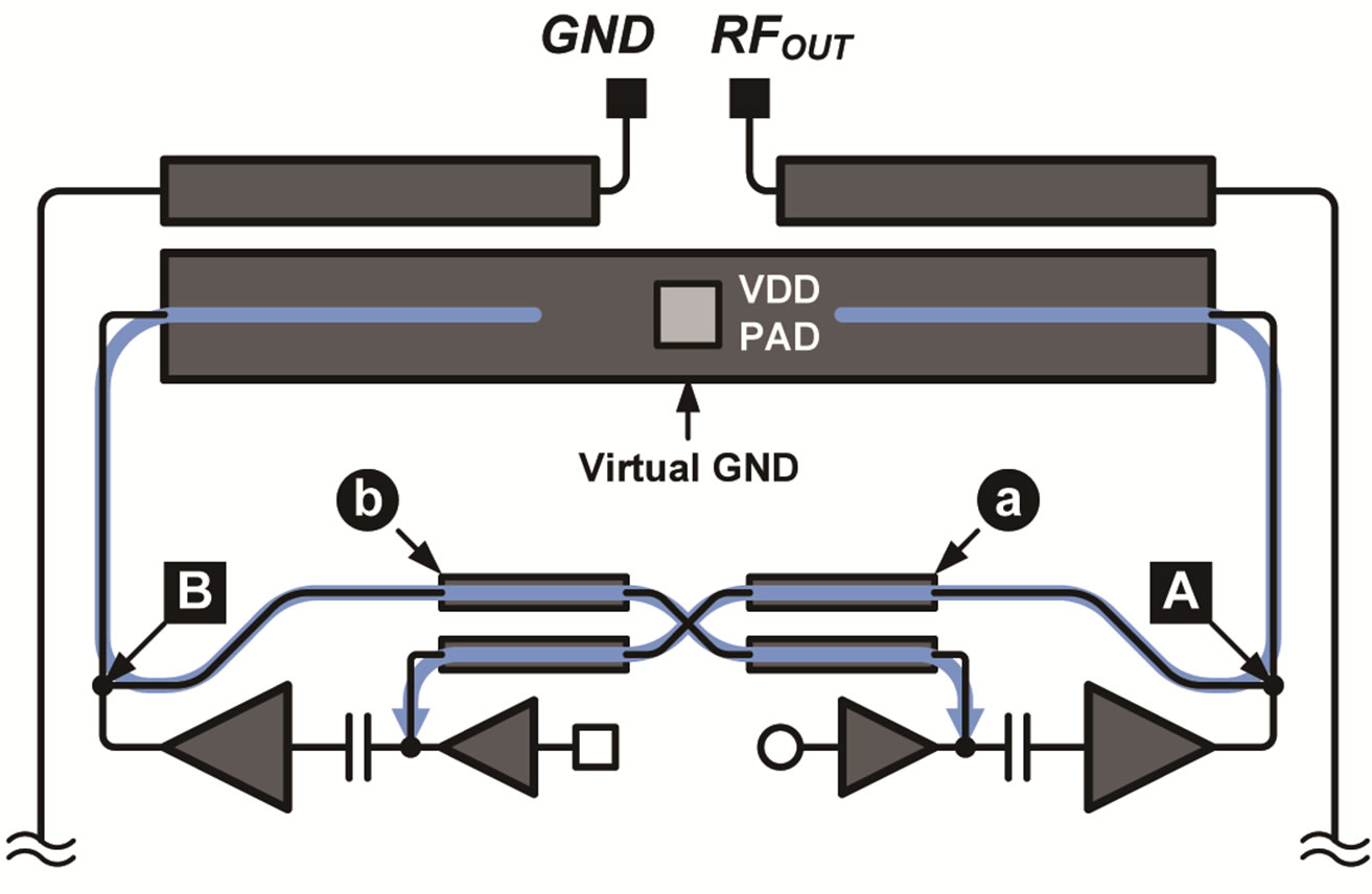
Figure 5 shows the proposed stage-convertible power amplifier. A distributed active transformer is used as an output power combiner, as this allows several problems associated with the output matching network for a CMOS power amplifier to be solved. Two differential pairs are used as the power stage and the driver stage for wattlevel maximum output power.
For low-power matching networks using differential line inductors, the layout and circuit architecture in Figures 3 and 4 must be modified, as shown in Figure 5. According to simulated and experimental results in earlier work [9], the inductance of a differential line inductor is approximately 1.75 times higher than that of a stand-alone line inductor. Thus, the quality factor of the differential line inductor is higher than that of the
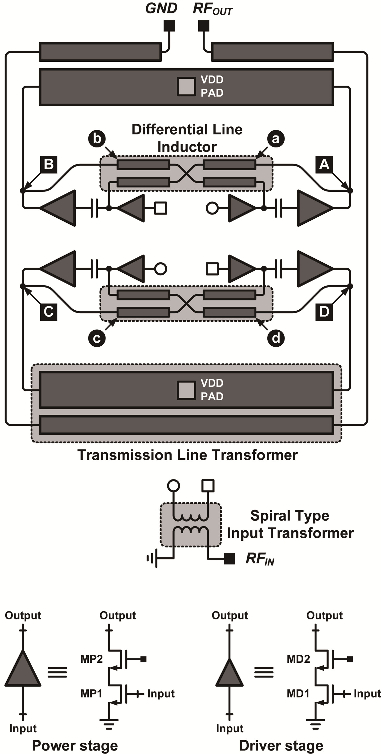
Figure 5. Stage-convertible power amplifier using the proposed differential line inductor [7,9].
stand-alone line inductor. However, the inductance of the differential line inductor can be controlled by adjusting the design parameters of the metal line width and the space between adjacent metal lines.
From the characteristics of the power amplifier using a distributed active transformer, the phases of A (or C) and B (or D) are out of phase, as shown in Figure 5, while the phases of A (or B) and C (or D) are in phase. Thus, the current directions of the line inductors of a (or c) and b (or d) are identical. Inductor a (or c) and b (or d) can therefore act as a differential line inductor. The inductance of the line inductor (a, b, c and d) is higher than that of a stand-alone line inductor when the length and width are identical to that of a differential line inductor.
In the stage-convertible power amplifier, the parasitic resistance of the low-power matching network should be minimized so as to improve the efficiency in the lowoutput power region effectively. In particular, minimizing the loss induced by the series inductor of the low-power matching network is most important. Thus, the differential line inductor is suitable for a low-power matching network because the inductance per unit length of the differential line inductor is higher than that of a conventional line inductor. Additionally, the proposed differential line inductor solves the size problems associated with conventional spiral-type inductors.
Figure 6 shows the RF current directions at the differential line inductor. As shown in Figure 6, the direction of the RF current through the adjacent transmission lines of the differential line inductor is always identical, which enhances the mutual inductance. The inductance of the differential line inductor can be designed using the space between lines “a” and “b” in Figure 6.
Figure 7 depicts the path along with the DC supply voltage enters the driver and power stages. As shown in Figure 7(a), the DC supply voltage enters the driver stage through the primary part of the transformer and the differential line inductor. The parasitic resistance induced by the differential line inductor needs to be minimized so as to maximize the efficiency in the low-power region. Additionally, because the power stage obtains its DC supply voltage through the low resistive primary part of the transformer, as shown in Figure 7(b), the efficiency in the high-power region can be maximized.
The differential line inductor thus becomes a solution for a stage-convertible power amplifier when used in a low-power matching network.
4. Design of the Proposed Power Amplifier
The key design parameter for the stage-convertible power amplifier is the low-power matching network, which ensures a high level of load impedance so as to improve the efficiency in the low-power region.
As described in the previous section, the low-power matching network is composed of series inductance and shunt capacitance to transform the low load impedance, RLOAD1, to the high load impedance RLOAD2. Figure 8
 (a)
(a)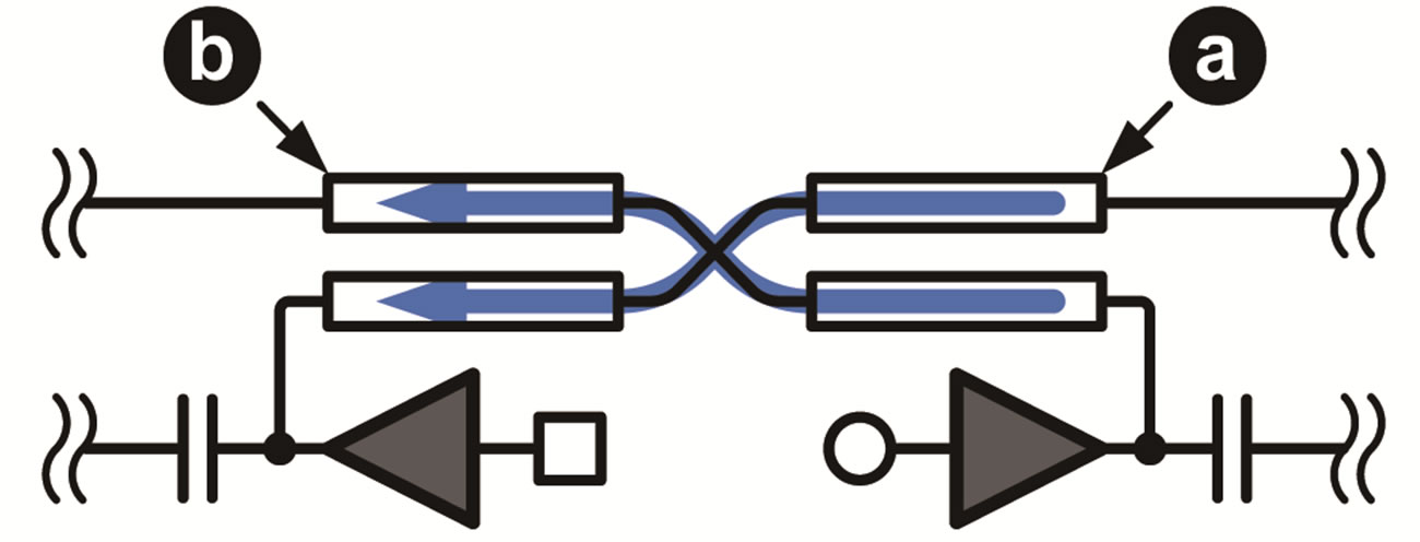 (b)
(b)
Figure 6. Stage-convertible power amplifier using the proposed differential line inductor.
 (a)
(a) (b)
(b)
Figure 7. Stage-convertible power amplifier using the proposed differential line inductor.
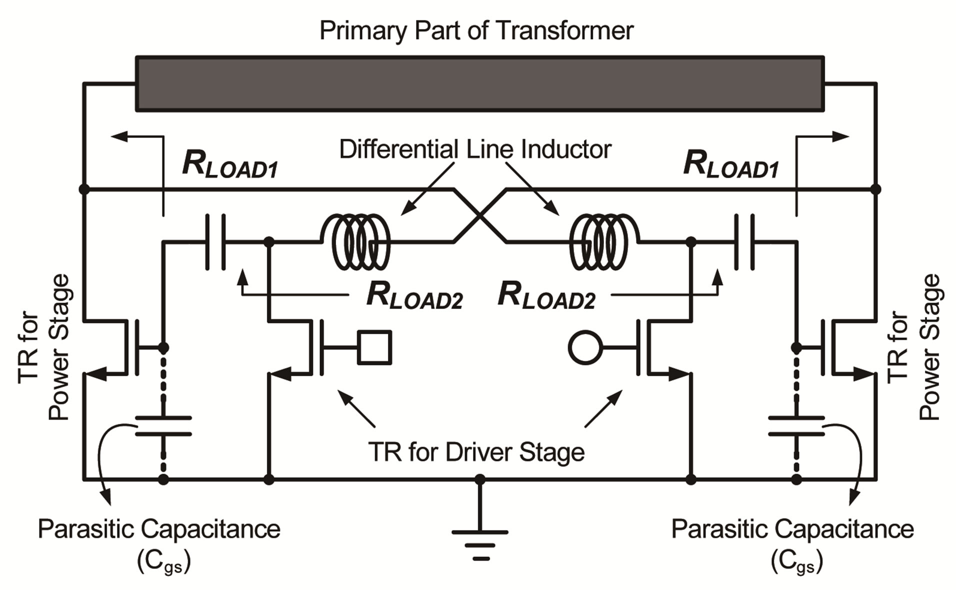
shows how the inductance and capacitance are transferred from the stage-convertible power amplifier using the differential line inductor. A simplified schematic of the amplifier shown in Figure 5 is depicted in Figure 8(a). The inductance of the differential line inductor is presented as the equivalent inductor. The parasitic capacitance of the transistor for the power stage, Cgs, becomes the shunt capacitance for the low-power matching network.
The equivalent circuit for the driver stage transistor and low-power matching network is shown in Figure 8(b). The parasitic capacitance, Cgs is determined by the transistor on-resistance of the power stage. If the determined Cgs is not sufficient for the successful design of the low-power matching network, an additional MIM shunt capacitor can be used. After the determination of the shunt capacitance, the required inductance of the differential line inductor can be calculated so as to obtain the desired load impedance RLOAD2, as shown in Figure 8(c). The inductance can be designed while controlling the metal width and the spaces between the adjacent transmission lines.
Earlier research contains an example of a stage-convertible power amplifier using a differential line inductor [7]. The power and driver stages are designed as a ClassE amplifier [10,11]. Among the various stage-convertible power amplifiers available, a low-power matching network using a differential line inductor is simplest and has the most compact size. The experimental results of the amplifier using the differential line inductor demonstrate the successful improvement of the efficiency in the low-power region.
 (a)
(a) (b)
(b)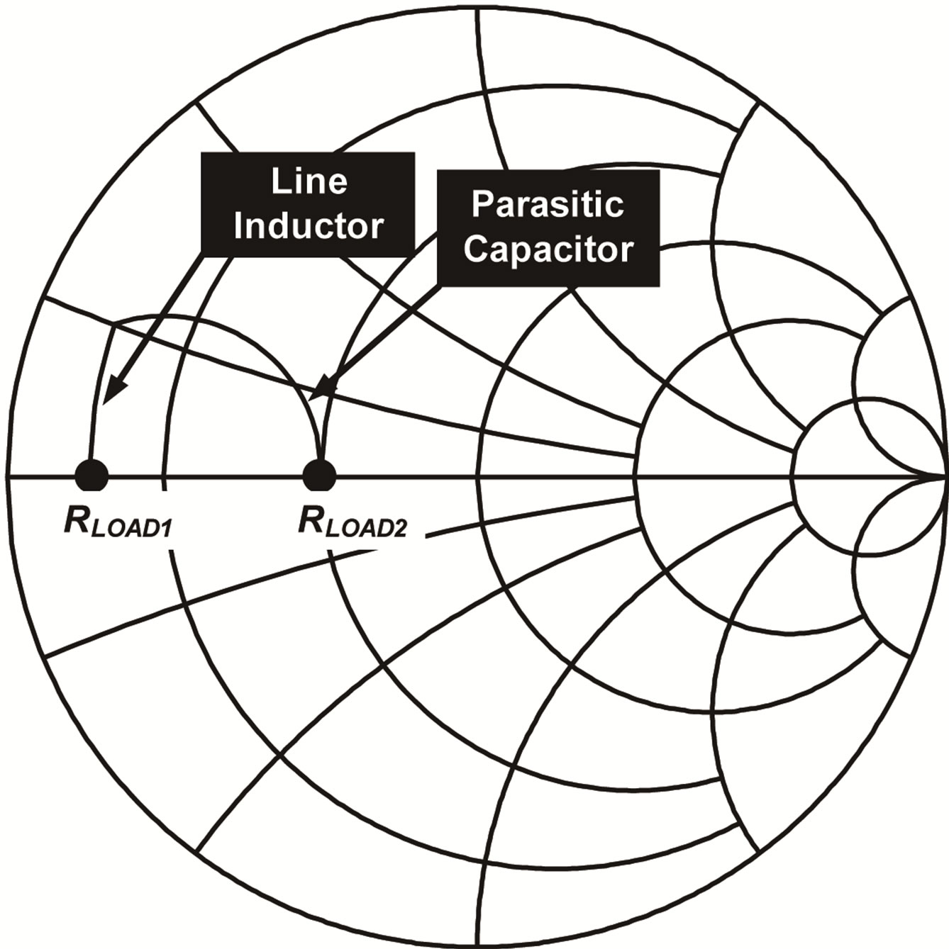 (c)
(c)
Figure 8. Block diagram of the stage-convertible power amplifier using a conventional line inductor.
5. Conclusions
In this review article, a differential line inductor and a stage-convertible RF power amplifier designed with the 0.18-mm RF CMOS process are described [7,9]. Among various low-power matching networks for a stage-convertible power amplifier, the differential line inductor is shown to be a suitable device in that it can enhance the efficiency and minimize the undesired coupling. In this review article, the design of a low-power matching network for a stage-convertible amplifier using a differential line inductor is explained. Additionally, the suitability of the differential line inductor for a matching network and the advantages of the differential line inductor are described.
In conclusion, the differential line inductor can solve the problems associated with the use of a stage-convertible amplifier, including the electric and magnetic coupling between the low-power matching network and the output matching network, the bulky characteristics of the matching network, and the low quality factor of a convention inductor.
6. Acknowledgements
This work was supported by Basic Science Research Program through the National Research Foundation of Korea (NRF) funded by the Ministry of Education, Science and Technology (2012-044627).
REFERENCES
- I. Aoki, S. D. Kee, D. B. Rutledge and A. Hajimiri, “Distributed Active Transformer—A New Power-Combining and Impedance-Transformation Technique,” IEEE Transactions on Microwave Theory and Techniques, Vol. 50, No. 1, 2002, pp. 316-331. doi:10.1109/22.981284
- I. Aoki, S. D. Kee, D. B. Rutledge and A. Hajimiri, “Fully Integrated CMOS Power Amplifier Design Using the Distributed Active-Transformer Architecture,” IEEE Journal of Solid-State Circuits, Vol. 37, No. 3, 2002, pp. 371-383. doi:10.1109/4.987090
- S. Kim, K. Lee, J. Lee, B. Kim, S. D. Kee, I. Aoki and D. B. Rutledge, “An Optimized Design of Distributed Active Transformer,” IEEE Transactions on Microwave Theory and Techniques, Vol. 53, No. 1, 2005, pp. 380-388. doi:10.1109/TMTT.2004.839940
- J. Staudinger, “Stage Bypassing in Multi-Stage PAs,” IEEE Transactions on Microwave Theory and Techniques, Symposium Workshop on Efficiency & Linearity Enhancement Methods for Portable RF/MW Power Amplifier, 2000.
- C. Park, Y. Kim, H. Kim and S. Hong, “A 1.9-GHz Triple-Mode Class-E Power Amplifier for a Polar Transmitter,” IEEE Microwave and Wireless Components Letters, Vol. 17, No. 2, 2007, pp. 148-150. doi:10.1109/LMWC.2006.890345
- C. Park, Y. Kim, H. Kim and S. Hong, “A 1.9-GHz CMOS Power Amplifier Using Three-Port Asymmetric Transmission Line Transformer for a Polar Transmitter,” IEEE Transactions on Microwave Theory and Techniques, Vol. 55, No. 2, 2007, pp. 230-238.
- C. Park, D. H. Lee, Y. Lee, J. Han, S.-H. Baek, Y. Kim and S. Hong, “1.8-GHz CMOS Power Amplifier with Stage-Convertible Structure Using Differential Line Inductor,” IEEE Radio Frequency Integrated Circuits Symposium, Digest of Papers, 2007, pp. 737-740.
- C. Park, D. H. Lee, Y. Lee, J. Han, S.-H. Baek, Y. Kim, and S. Hong, “A 1.8-GHz CMOS Power Amplifier Using a Dual-Primary Transformer with Improved Efficiency in the Low Power Region,” Radio Frequency Integrated Circuits (RFIC) Symposium Vol. 56, No. 4, 2008, pp. 782-292. doi:10.1109/TMTT.2008.918152
- C. Park, “Experimental Investigation of Differential Line Inductor for RF Circuits with Differential Structure,” International Journal of Maritime Information and Communication Sciences, Vol. 9, No. 1, 2011, pp. 11-15.
- N. O. Sokal and A. D. Sokal, “Class-E: A New Class of High-Efficiency Tuned Single-Ended Switching Power Amplifiers,” IEEE Journal of Solid-State Circuits, Vol. 10, No. 3, 1975, pp. 168-176. doi:10.1109/JSSC.1975.1050582
- S. H.-L. Tu, “A Power-Adaptive CMOS Class E RF Tuned Power Amplifier for Wireless Communications,” Proceedings of IEEE International SOC Conference, 17- 20 September 2003, pp. 365-368.