Wireless Engineering and Technology
Vol.3 No.3(2012), Article ID:21458,4 pages DOI:10.4236/wet.2012.33016
A Wideband Circularly Polarized Patch Antenna for 60 GHz Wireless Communications
![]()
1Department of Electrical and Computer Engineering, The University of Arizona, Tucson, USA; 2IBM T. J. Watson Research Center, New York, USA.
Email: rgzhou2012@gmail.com, hxin@ece.arizona.edu
Received May 5th, 2012; revised June 2nd, 2012; accepted June 10th, 2012
Keywords: Patch Antenna; Circular Polarization; Millimeter Wave; Wireless Communication
ABSTRACT
This paper presents the design of a fully packaged 60 GHz wideband patch antenna incorporating an air cavity and a fused silica superstrate. Circular polarization (CP) is realized by introducing a diagonal slot at the center of the square patch. By optimizing the patch and the slot dimensions, a high efficiency (>90%) microstrip fed CP antenna with an impedance bandwidth of 24% and a 6 dB axial ratio bandwidth of 21.5% is designed. A coplanar waveguide (CPW) to microstrip transition with λ/4-open-ended stubs are then designed to match the antenna to the CPW packaging interface. The experimental results of the final packaged antenna agree reasonably with the simulation results, demonstrating an impedance bandwidth of more than 26% and a 6 dB axial ratio bandwidth of 22.7%.
1. Introduction
Demands of modern communication and sensor systems for more bandwidth, higher resolution and compactness lead to operating frequency up to the millimeter wave (mmWave, f > 30 GHz) or even sub-mmWave regime. In particular, the 60 GHz ISM (the industrial, scientific and medical) band is available in many countries. For example, in the US, the ISM band spans from 57 to 64 GHz with a worldwide overlap of 5 GHz of bandwidth for unlicensed use. As a result of the large bandwidth available, the 60 GHz band is very attractive for a number of applications, including wireless personal-area networks (WPAN) and local-area networks (WLAN). As the battery lifetime is a major bottleneck for many portable devices, the 60 GHz band has a distinct benefit because the large bandwidth can be utilized to tradeoff bandwidth efficiency for low power consumption, while still maintaining high data rate [1]. In addition, due to the atmospheric absorption (mainly oxygen molecules) peak around 60 GHz, communication link at this band is inherently secure and has less interference among users, which are ideal for indoor applications. However, at mmWave frequencies, higher material losses, fabrication tolerances and packaging issues often hinder the performance of wireless front-ends. Therefore, as an important front-end component, mmWave antennas that are wideband, efficient and packaged to be compatible with integrated circuits are highly desirable. Moreover, previous wireless channel propagation studies have shown that circular polarization can effectively suppress multi-path fading and inter-symbol interference (ISI) [2-4].
Various techniques to improve antenna performances such as bandwidth and efficiency have been reported in the literature. As shown in [5], cavity backing can isolate an antenna from its surroundings, suppress surface waves and increase antenna bandwidth. The detailed characteristics of various cavity backed antennas are summarized in [6]. Another approach to improve the bandwidth and efficiency of the conventional patch antenna is to minimize the substrate dielectric constant, as demonstrated in [7,8]. It is also known that the antenna gain can be considerably increased by covering the antenna with a high permittivity superstrate [9,10]. The fundamental effects of the substrate-superstrate structure on printed-circuit antennas are explored in [11], demonstrating that the antenna radiation efficiency can be optimized to approximately 100% by selecting the proper materials and dimensions of the substrate and superstrate.
All of the above mentioned techniques for improving the antenna performances can be applied in the mmWave antenna design. Several cavity backed wide-band antennas have been demonstrated in the V-band in [12-16]. In addition, metamaterial/EBG (electromagnetic band gap) based antennas with increased antenna gain have been reported in [17-21]. A good review of various mmWave integrated circuit antennas can be found in [22]. Furthermore, several topologies of circularly polarized antenna have been proposed for the 60 GHz wireless communications [23-28].
In this paper, we present the detailed design of a 60 GHz left-hand circular polarized antenna [27] that has a good overall performance by combining various techniques reported in [5-16,29-31]. This patch antenna incorporates a diagonal slot at the center and features a superstrate and an air cavity backing to achieve desired performances including wide bandwidth, high efficiency and low axial ratio. The metal frame underneath the antenna layer serves as the cavity backing, useful for antenna bandwidth enhancement, as well as mechanical support for the antenna, making the antenna much more stable than using a supporting pin (only feasible at low frequencies) [7]. The microstrip-fed patch antenna is packaged with a flip-chip CPW interface that is fully compatible to semiconductor integrated circuits (ICs). In [29-31], linear polarized folded dipole antennas for 60 GHz applications using this superstrate/substrate topology and packaging scheme have been demonstrated. In this work, by optimizing the slot length of the patch antenna, a 6 dB axial ratio bandwidth of 22.7% is achieved, which is much greater than the 1.1% axial ratio bandwidth in [32]. Moreover, this antenna achieves a wide bandwidth of more than 26%.
A prototype antenna is fabricated and characterized using a probe-based measurement setup as described in [29]. The demonstrated patch has a dimension of 1050 mm × 1050 mm, while the final packaged antenna including feed lines has a dimension of 4849 mm × 5555 mm. Beyond the initial report in [27], the detailed design procedure of the circularly polarized antenna, including the design of the microstrip-fed patch antenna and the comparison of the performances of the antenna with different feeding interfaces, is described in this paper. The measured antenna efficiency is also obtained, demonstrating greater than 75% efficiency over the entire measured frequency range. In addition, the measured co-polarized and cross-polarized radiation patterns of the antenna are presented and compared with simulation predictions. Discussions on the measurement uncertainties that may explain the simulation/measurement discrepancies are included.
This paper is organized as the following. Section 2 introduces the antenna structures including its packaging. Section 3 describes the detailed antenna design procedures. The simulated (by finite-element electromagnetic solver HFSS) and measured antenna properties are compared in Section 4.
2. Antenna Structure/Packaging
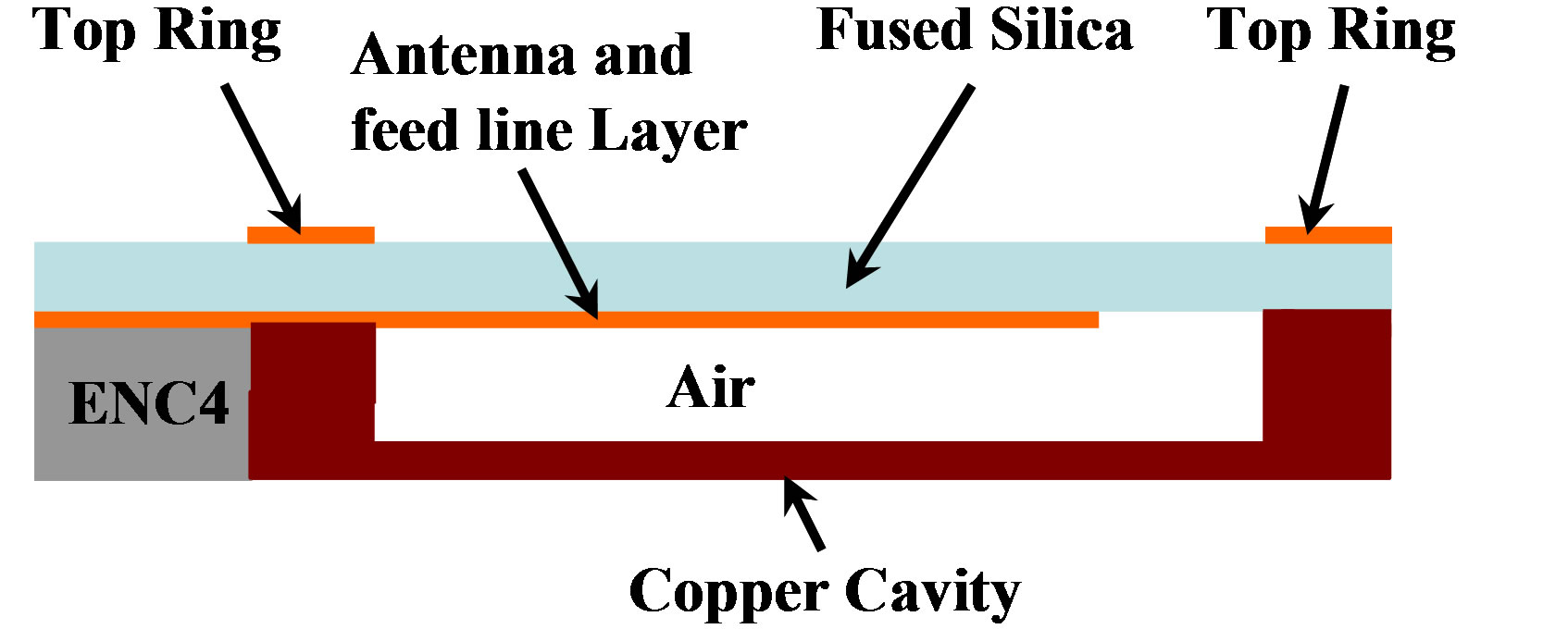
Since packaging at mmWave frequency is challenging and critical to system performance [30], mmWave antenna designs should incorporate the packaging aspects as early as possible. The geometry of the entire antenna structure including its packaging is shown in Figure 1(a), which consists of a top fused silica substrate (superstrate), a bottom air cavity made of copper and dielectric sealant encapsulant with a dielectric constant of 4 (ENC4) for further integration with flip-chipped ICs [30]. Similar package structures have been applied previously for folded dipole antennas and more detailed package design information can be found in [30,31]. The applied cavity size is optimized according to the antenna impedance bandwidth. The superstrate thickness T = 300 µm is a compromise since thinner fused silica samples would be difficult to manufacture and a thicker superstrate leads to reduced efficiency due to more energy staying in the dielectric layer as surface waves. All of the metallization (2 mm thick gold) of the patch antenna and its feed lines is on the lower side of the fused silica substrate, which has negligible loss tangent at 60 GHz and a relatively low dielectric constant of 3.8. To minimize the surface wave effects that can affect the radiation in the antenna plane, a gold ring is placed on the upper side of the fused silica. The fused silica substrate is mounted on top of an air cavity with copper walls, as shown in Figure 1(b). The cavity has an internal size of 3890 mm × 3849 mm and an external size of 4890 mm × 4849 mm. The cavity height
 (a)
(a)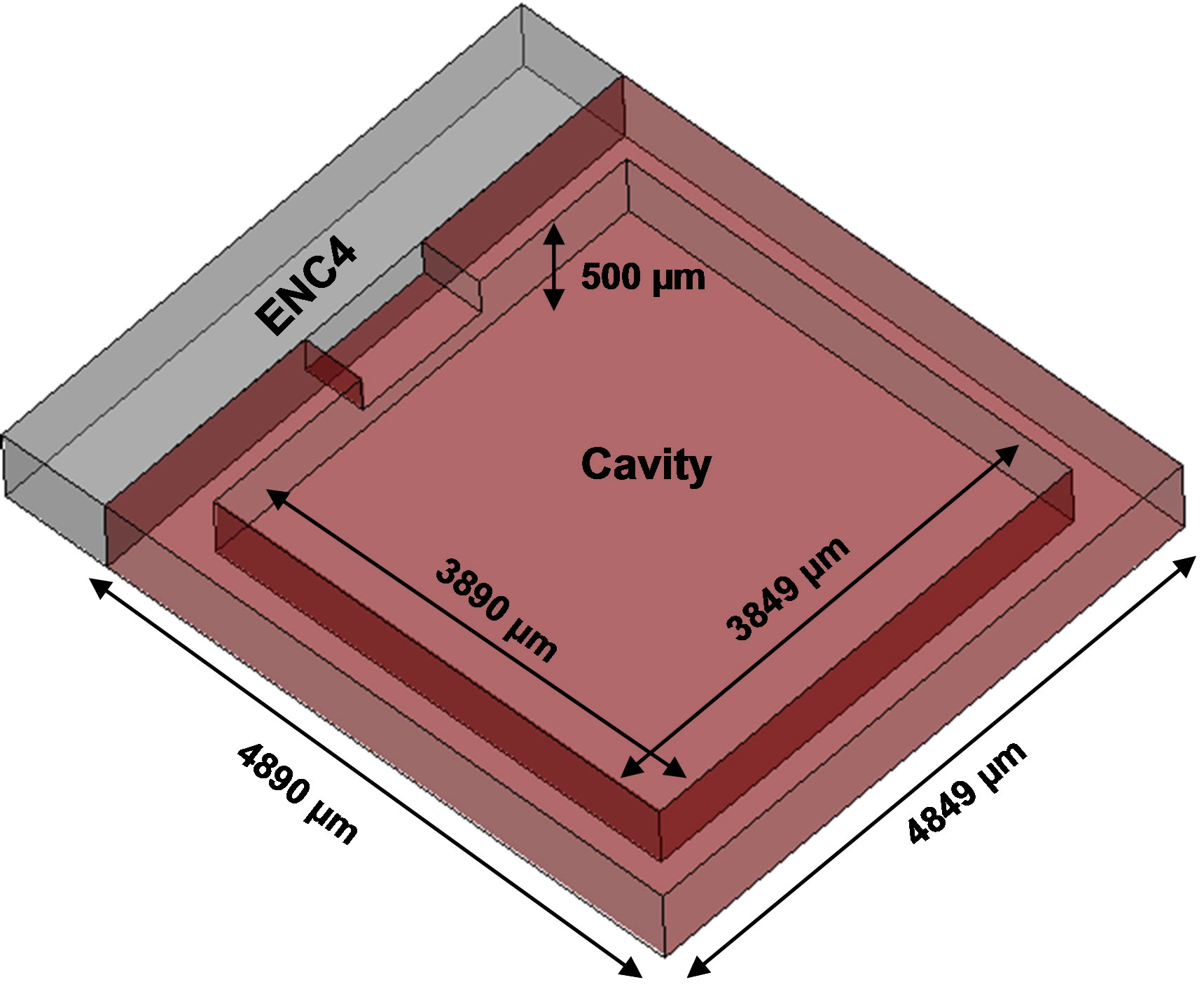 (b)
(b)
Figure 1. (a) The side view of the entire antenna structure; (b) The copper cavity.
is 500 mm, being the trade-off between the package size and the antenna bandwidth. The detailed parameters of the antenna structure and packaging are listed in Table 1.
The antenna structure shown in Figure 1 has several advantages. First, a patch antenna at the lower side of the fused silica can be thought as having an air substrate with a dielectric constant of 1 and a superstrate with a dielectric constant of 3.8. These will lead to significant bandwidth and efficiency improvements compared with a normal one substrate patch antenna. In [31], a broadband dipole antenna for 60 GHz applications using a similar cavity and superstrate was reported. Second, this packaging scheme is fully compatible with flip-chip mounted monolithic integrated circuits such as an entire SiGe transceiver [30]. A schematic of the antenna flip-chip integrated with an IC chipset is shown in Figure 2.
3. Detailed Antenna Design
For the initial design, a microstrip-fed square patch antenna with a diagonal slot is applied to achieve left-hand circular polarization [32,33], as shown in Figure 3. The patch size is first selected to obtain a resonant frequency around 61 GHz and the microstrip line width is tuned to match the antenna impedance. The slot length mainly controls the circular polarization performance. It is observed that the frequency at which the axial ratio is minimum increases when the slot length C increases (10 GHz when C = L/2, 51 GHz when C = L/1.1 and 75 GHz when C = L/0.9), with the fixed patch size of 1400 µm and the slot width d kept at C/10 [34]. In addition, it is found that the slot length C also influences the antenna

Table 1. Configuration of the antenna structure and packaging.
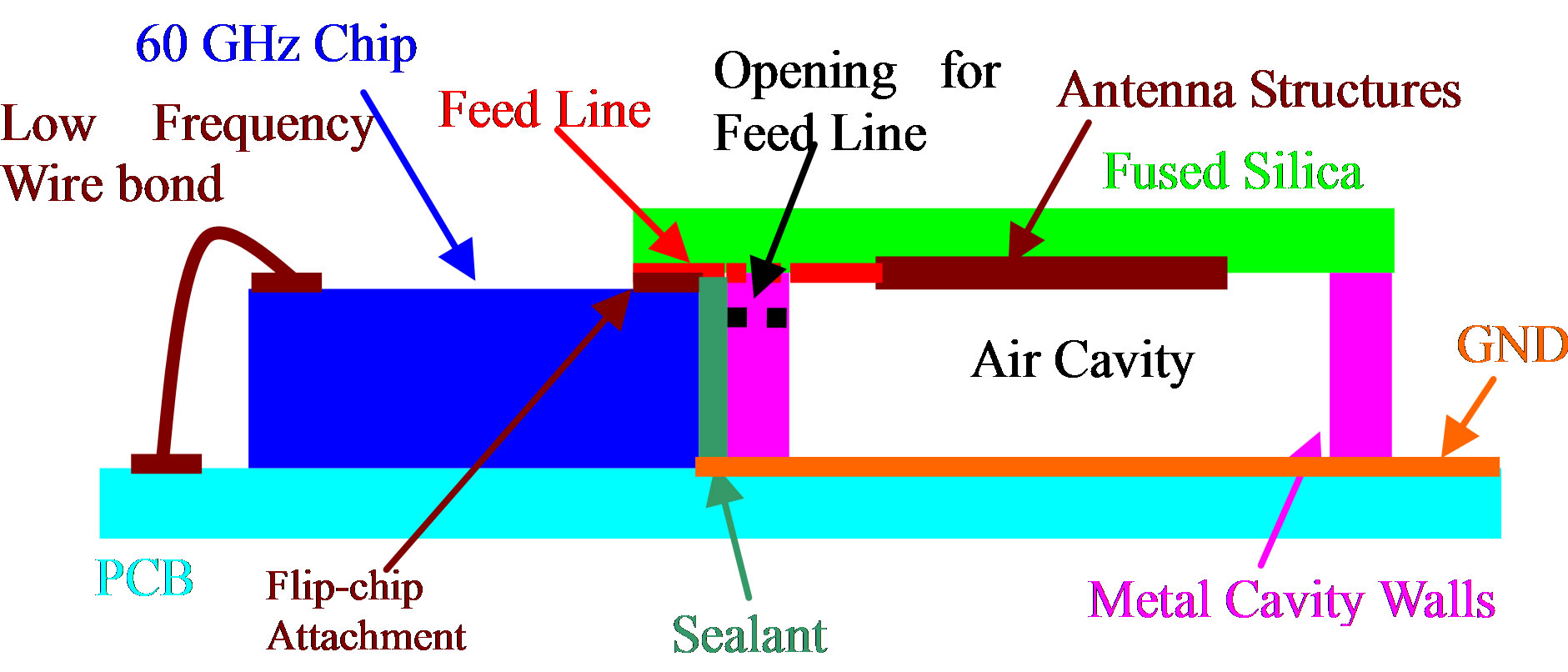
Figure 2. Schematic view of the antenna packaged with an integrated chipset.
resonance frequency: the resonance frequency decreases when the slot length increases (with the fixed patch size and the slot width kept at C/10). Figure 4 compares the simulated antenna reflection coefficients (S11 in dB) for different slot lengths with the square patch size L = 1400 µm. The antenna resonance frequency shifts from 62 GHz to 57 GHz when the slot length C increases from L/2 to L/0.9. The final dimensions of the patch antenna are optimized to make both the resonant frequency and the frequency with the minimum axial ratio at 61 GHz. The finalized design parameters are listed in Table 2.
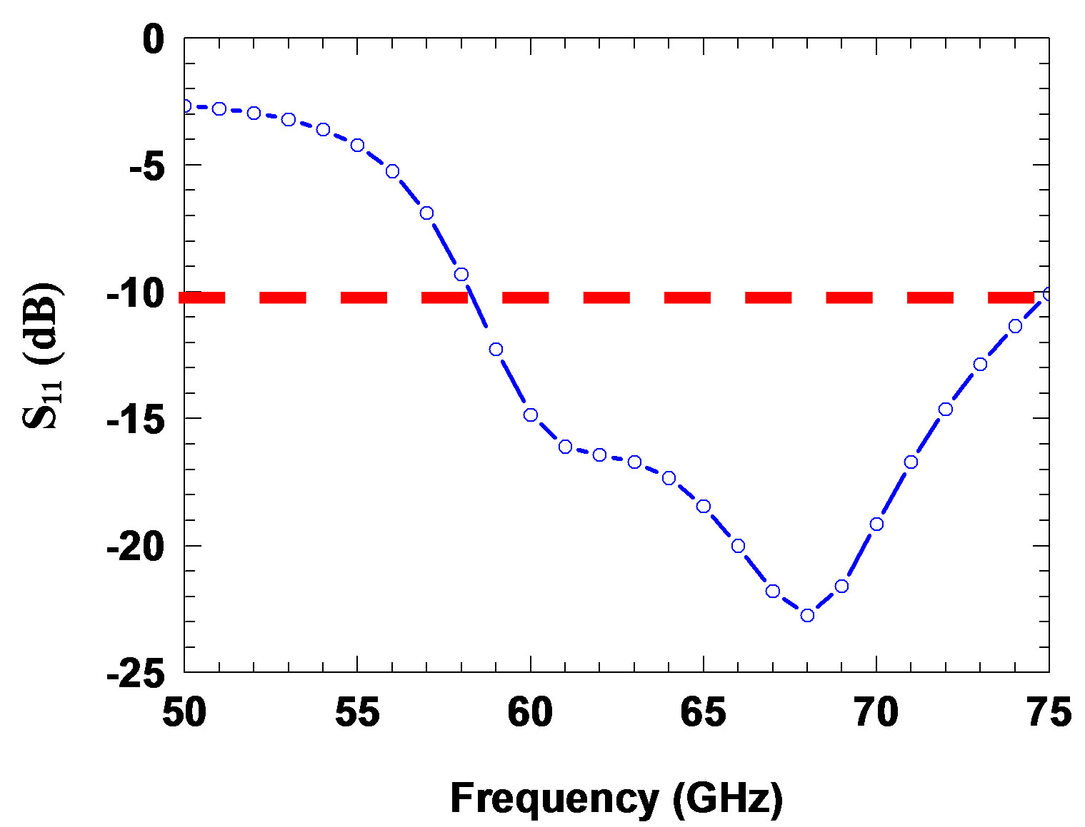
The simulated reflection coefficients (S11 in dB) and axial ratio of the optimized antenna are plotted in Figure 5. It can be seen that S11 is less than –10 dB from 59 GHz to 75 GHz, with a bandwidth of about 24%. The axial
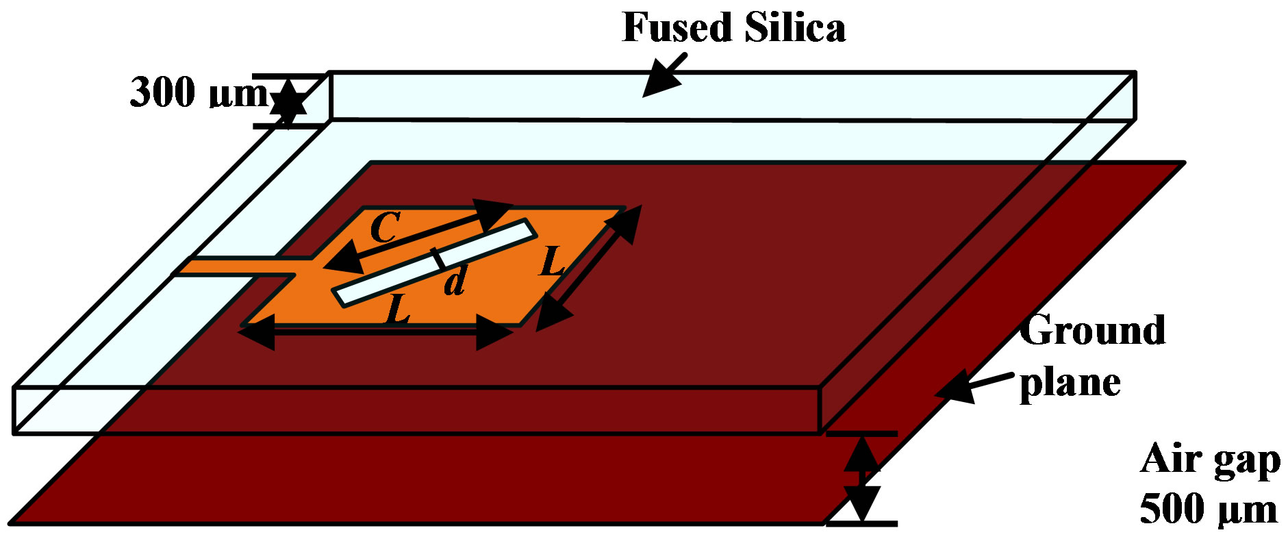
Figure 3. The microstrip-fed square patch antenna with a diagonal slot.
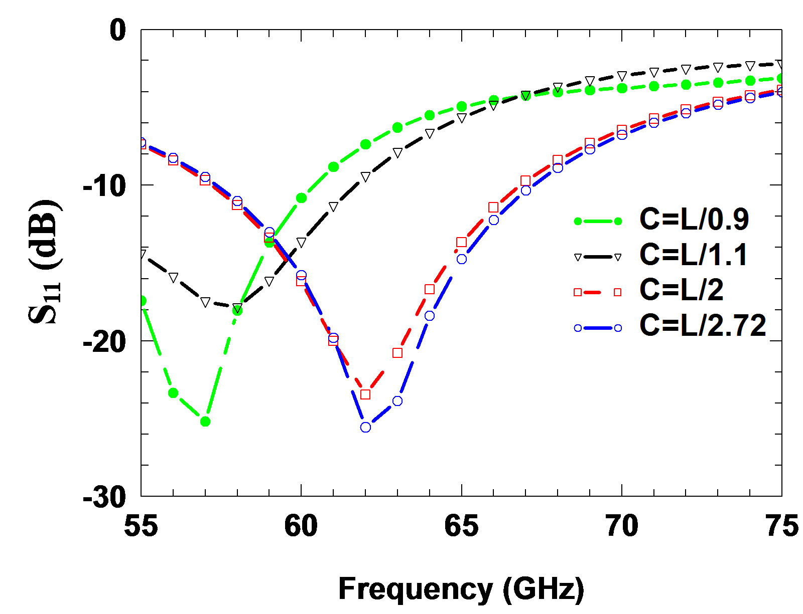
Figure 4. Simulated reflection coefficients (S11 in dB) of the square patch antenna (L = 1400 µm) with different slot lengths C (slot width d = C/10).
Table 2. The dimension of the finalized patch antenna design.
 (a)
(a)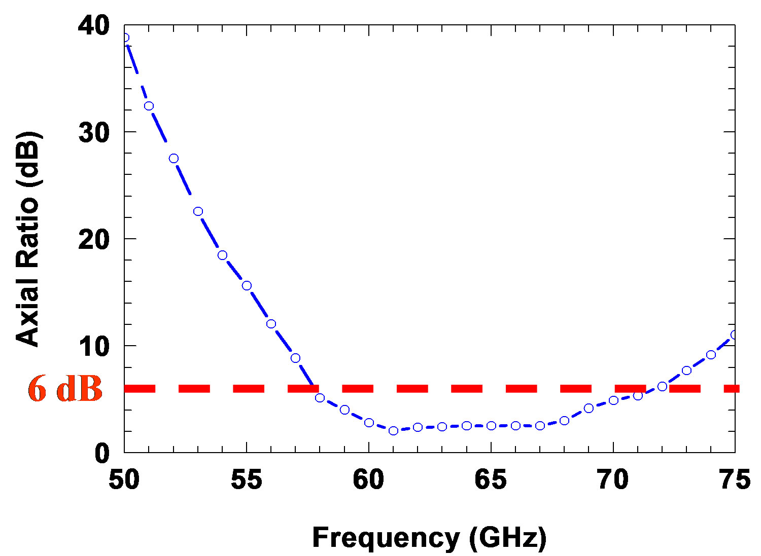 (a)
(a)
Figure 5. Simulated microstrip-fed square patch antenna performance: (a) Reflection coefficients (S11 in dB); (b) Axial ratio.
ratio is less than 6 dB from 58 GHz to 72 GHz, with a bandwidth of 21.5%. Comparing with conventional patch antennas, the bandwidth of the optimized antenna is much greater due to the utilization of the air cavity and the fused silica superstrate. The simulated antenna efficiency is higher than 90% for the entire frequency range from 50 to 75 GHz.
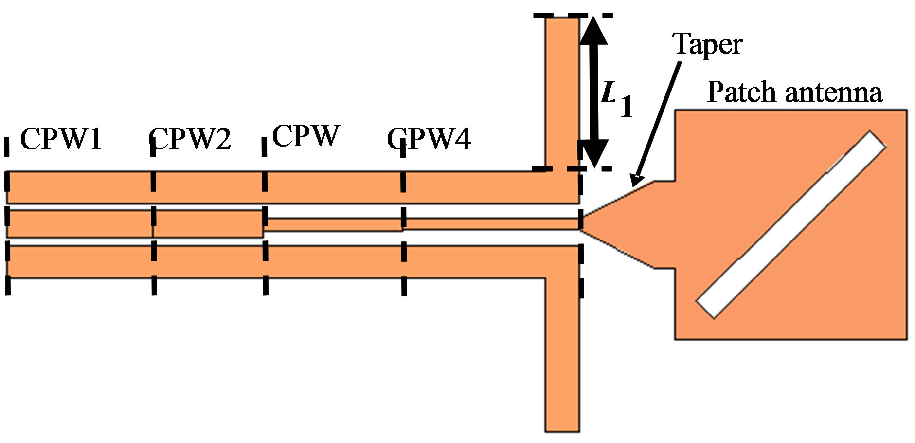
A CPW to microstrip transition is then designed to satisfy the CPW interface of the antenna packaging and enable convenient measurements using a CPW probe. The transition section is composed of a tapered microstrip line and a CPW line (labeled CPW4) with two approximately λ/4 open-stubs to achieve the desired grounding at the transition [35] around the center frequency of 61 GHz, as shown in Figure 6(a) with straight open stubs and Figure 6(b) with bent open stubs. The CPW4 section is designed to have the same impedance (102 Ω) as the microstrip. Two additional CPW lines (labeled CPW3 and CPW2) are used to transform the 102 Ω CPW line (CPW4) to the input 50 Ω CPW line (labeled CPW1).
To evaluate the impact of the CPW packaging, the HFSS simulated performances of the antennas with direct microstrip feeding, the CPW feeding with the straight open-stubs and the bent open-stubs are compared in
 (a)
(a)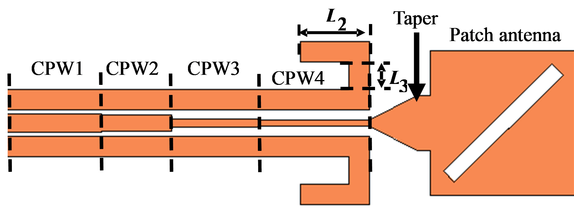 (b)
(b)
Figure 6. The top view of the antenna layer including (a) The CPW feed with straight open-stubs; (b) The CPW feed with bent open-stubs.
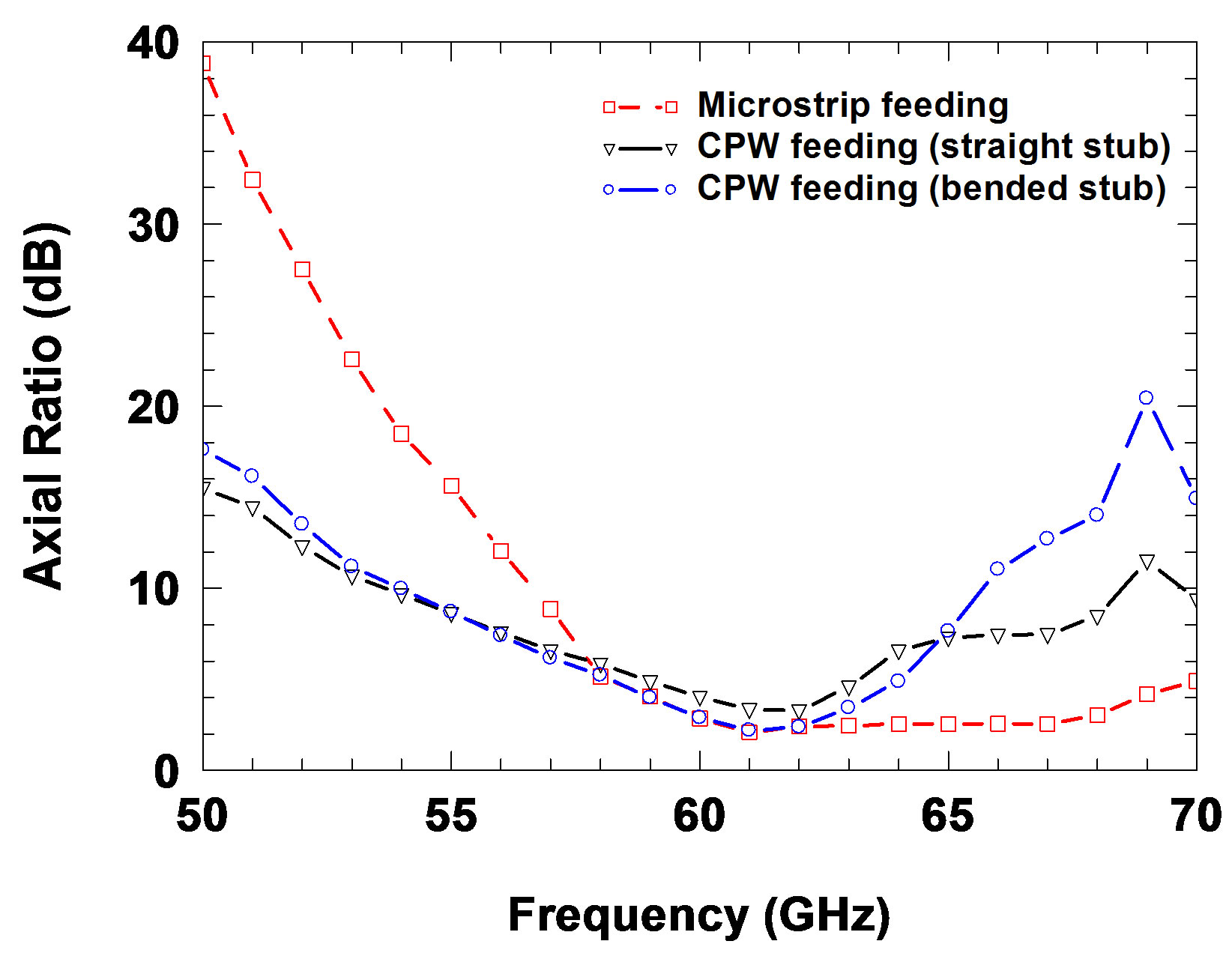
Figure 7. The simulated antenna efficiencies are greater than 90% for all the cases. The reflection coefficients and axial ratios of the three cases are similar at frequencies around 61 GHz (58 GHz - 64 GHz), as expected. With the CPW feeding sections, the antenna has a wider bandwidth and a narrower axial ratio bandwidth compared to those of the direct microstrip feeding. The S11 of the antennas with the CPW feedings are less than 10 dB from 50 GHz to 70 GHz with a bandwidth of 33%, which are larger than the 17% bandwidth of the antenna with the microstrip feeding. The 6 dB axial ratio bandwidths of the antennas with the microstrip feeding, the CPW feeding with straight open-stubs and bent open-stubs are 18.7%, 9%, and 9.9%, respectively. In combination, the bandwidth with both S11 less than –10 dB and axial ratio less than 6 dB drops from 17% to 9% and 9.9% when the CPW feeding sections are added to match the CPW interface, which is still sufficient for the applications at 60 GHz. In addition, the axial ratios of the antenna with bent open-stubs are around 1 dB lower than the case with straight open-stubs at frequencies around 61 GHz. Therefore, to reduce the impact of the λ/4 open-stubs on the radiation characteristics (especially the axial ratio) of the antenna, the bent λ/4 open-stubs are used for the final design. The final dimensions of the feeding sections are listed in Table 3, where L is the transmission line length, W is the transmission line width, g is the CPW gap, W1 and W2 are the widths of the two ends of the tapered mirostrip. The widths of the two CPW grounds are 150 um each.
 (a)
(a)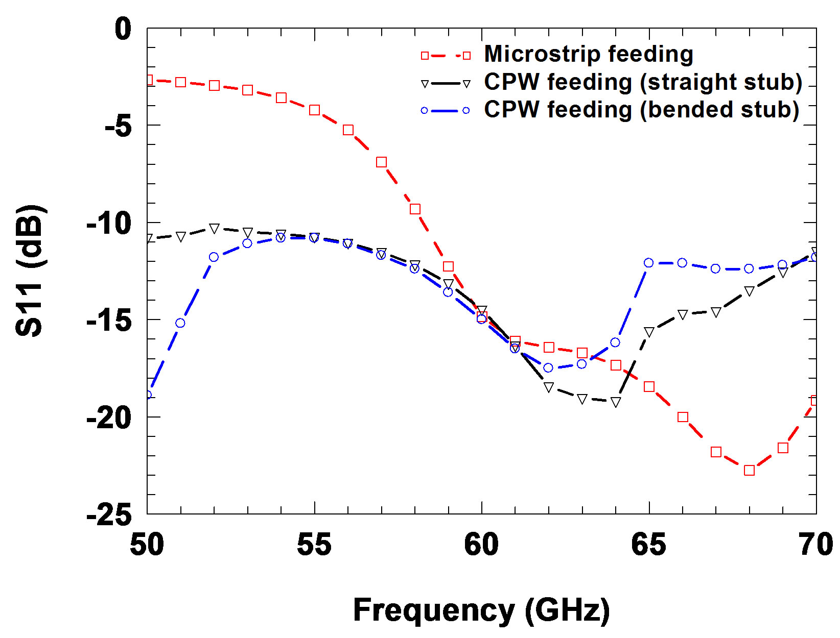 (b)
(b)
Figure 7. Comparison of antennas with different feedings (a) the axial ratio (b) the reflection coefficient (S11 in dB).
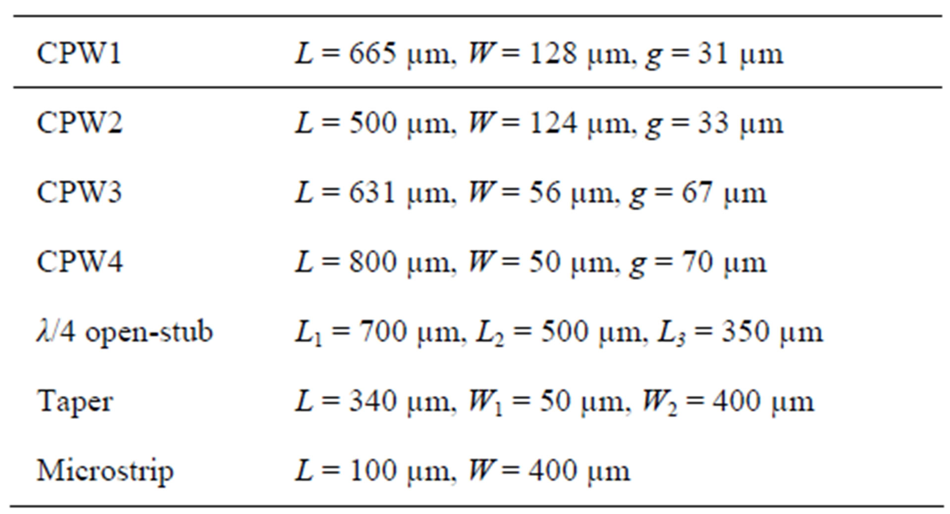
Table 3. The geometry of the CPW to microstrip transition.
4. Comparison of Measurement and Simulation
To validate the performances of the designed 60 GHz left-hand circular polarized antenna, a prototype is fabricated by a thin-film resolution metal patterning process. The detailed fabrication procedure can be found in [30,31]. Figure 8 shows a photo of the fabricated and packaged antenna. Note that the antenna layer on the bottom side of the fused silica can be clearly seen because of the transparency of the fused silica superstrate.
The antenna performances including return loss, axial ratio, gain and radiation pattern are characterized from 50 GHz to 65 GHz using a CPW probe based measurement setup in an anechoic chamber, as it is described in detail in [29]. To measure the axial ratio of the fabricated antenna, both a straight and a twisted waveguide adapter are used to feed the receiving standard gain horn. The challenge of the axial ratio measurement at 60 GHz is that it is very sensitive to the phases of the two polarizations. For example, when the straight waveguide adapter is replaced by the twisted one or vice versa, small misalignment would lead to the inaccuracy of the measured axial ratio.
Figure 9 plots the simulated and measured S11 of the fully packaged antenna (reference point at the beginning of the CPW line). The measured result indicates a 10 dB bandwidth greater than 26% (limited by the experimental frequency range), agreeing well with the simulation result. The measured axial ratio is plotted in Figure 10,
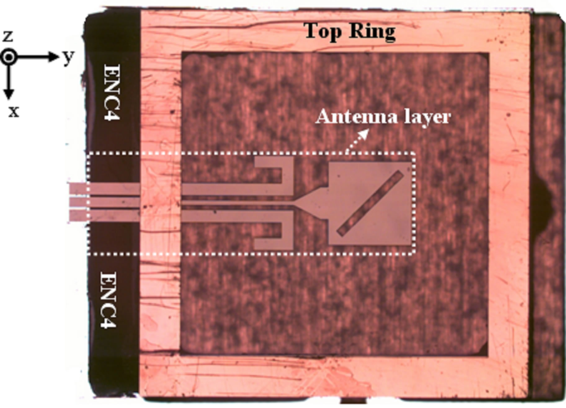
Figure 8. A photo showing the top view of the fabricated and packaged 60 GHz left-hand circular polarized patch antenna.
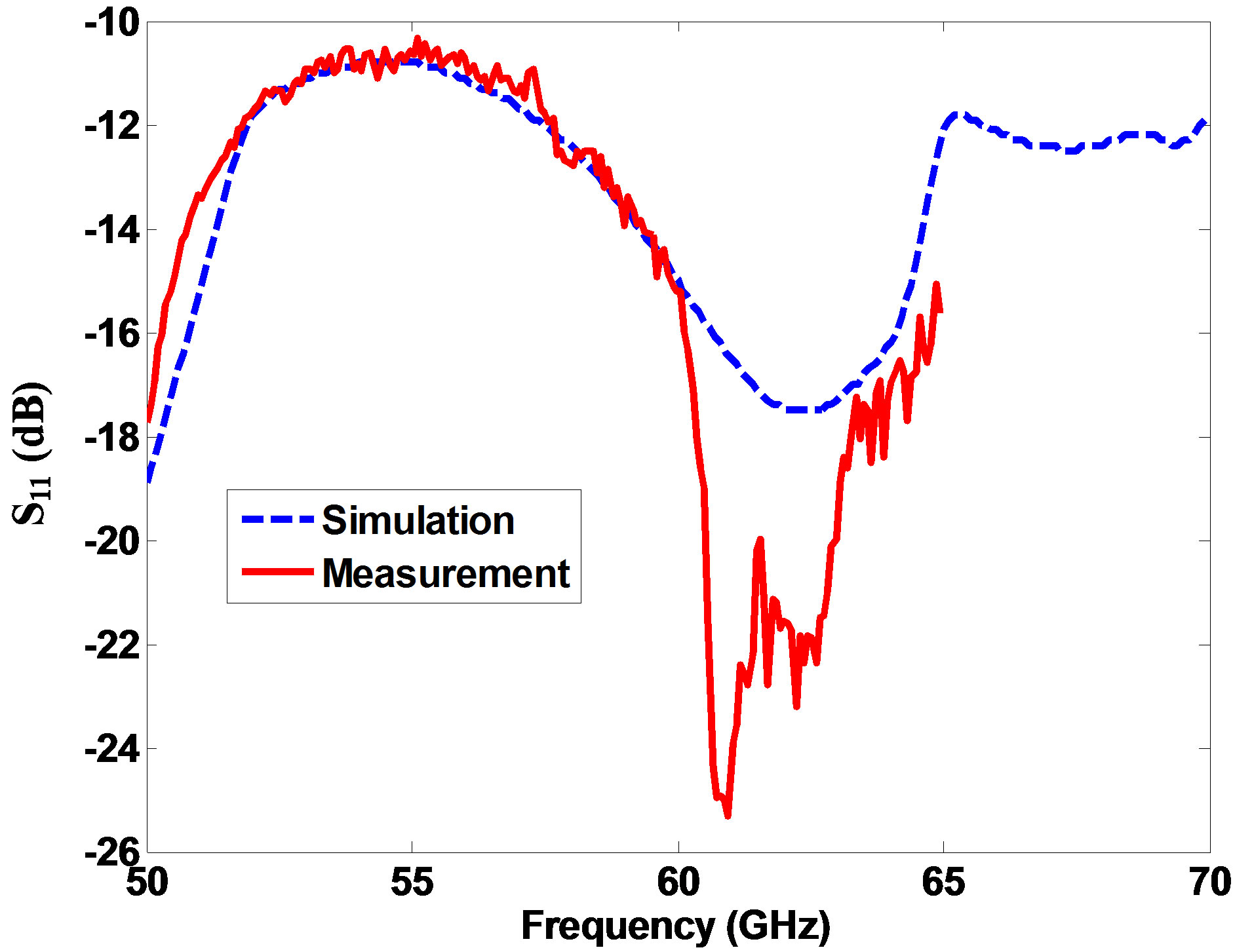
Figure 9. The simulated and measured reflection coefficients (S11 in dB) of the fully packaged antenna.
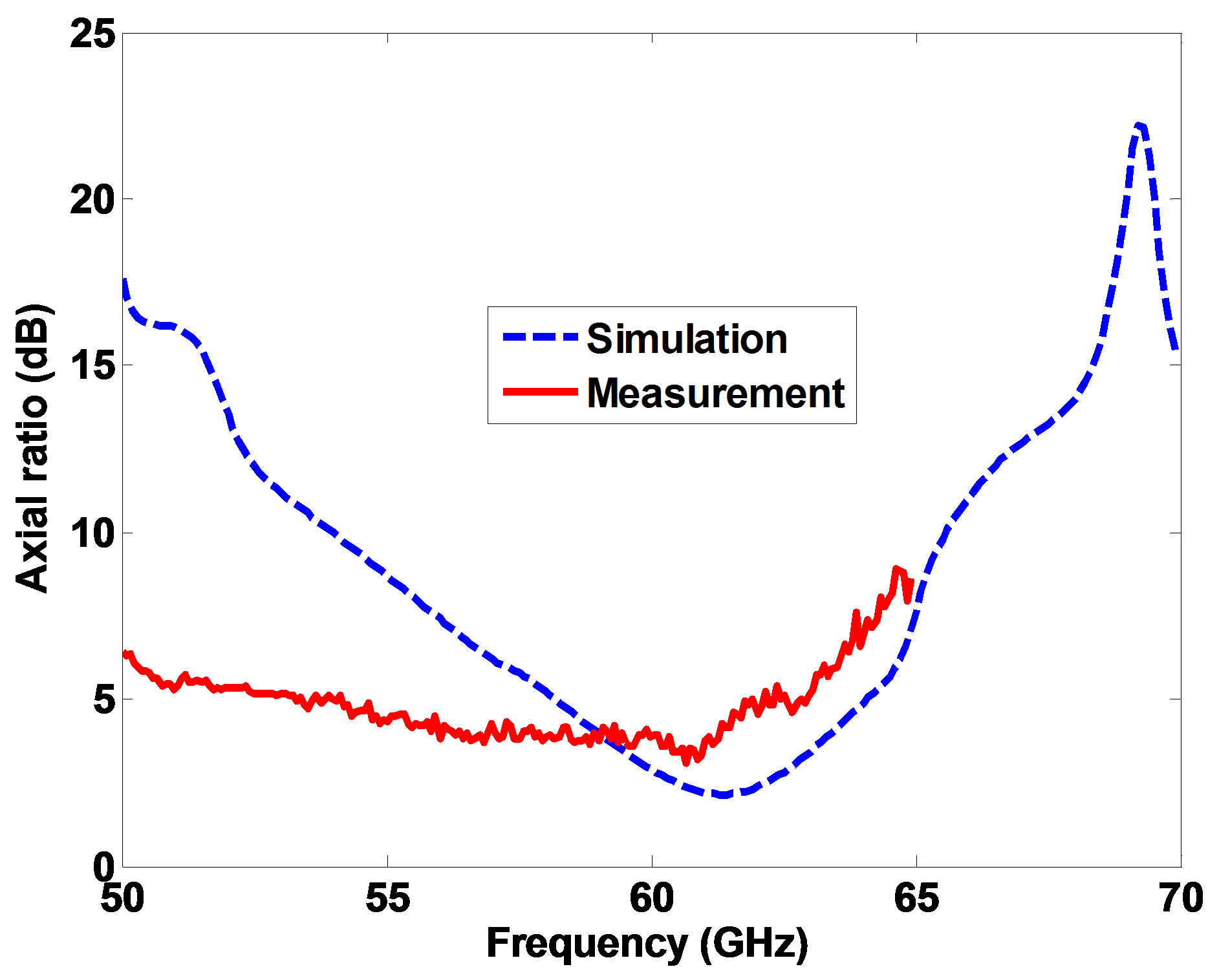
Figure 10. The simulated and measured axial ratio of the fully packaged antenna.
together with the simulated result. The simulated 6 dB axial ratio bandwidth is 9.9%, with a minimum value of 2.7 dB at 61 GHz. The measured minimum axial ratio (3.0 dB) also occurs around 61 GHz and the 6 dB axial ratio bandwidth is 22.7%. The measurement and simulation results agree well above 60 GHz but the measured values are significantly smaller at the lower frequencies. The discrepancy between the simulated and measured axial ratios is likely due to the measurement uncertainties discussed previously.
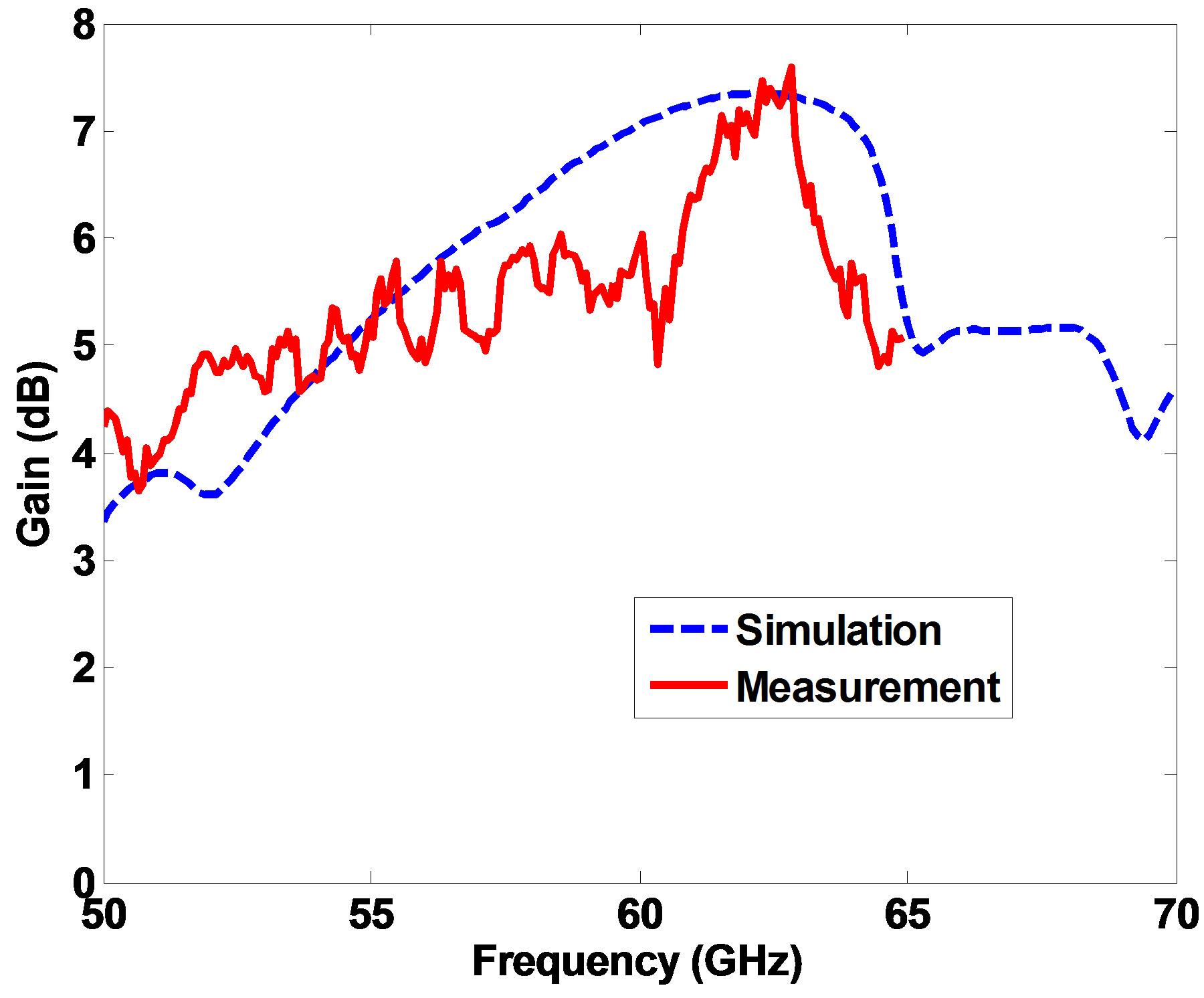
The radiation characteristics of the antenna are measured in both x-z and y-z planes (see Figure 8). The simulated and measured antenna gains (x-z plane) as a function of frequency are shown in Figure 11(a). They match reasonably well with each other near the center frequency (at 61 GHz, the measured and simulated gains are 6.4 dB and 7.3 dB, respectively). The measured gain in the y-z plane (not shown) also has similar shape and range but is distorted a bit due to the interference of the antenna feeds in the measurement. Our simulation shows that the antenna efficiency is greater than 90% within the simulated frequency range, as the dashed curve plotted in Figure 11(b). The measured antenna efficiency ηmea is then estimated as: 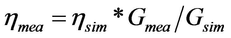 (with the assumption that the measured and simulated directivities are consistent), where
  is the simulated antenna efficiency,
  and
and  are the simulated and measured antenna gains, respectively. It can be seen from Figure 11(b) that the measured efficiency (solid curve) varies from 75% to 92% from 57 to 64 GHz.
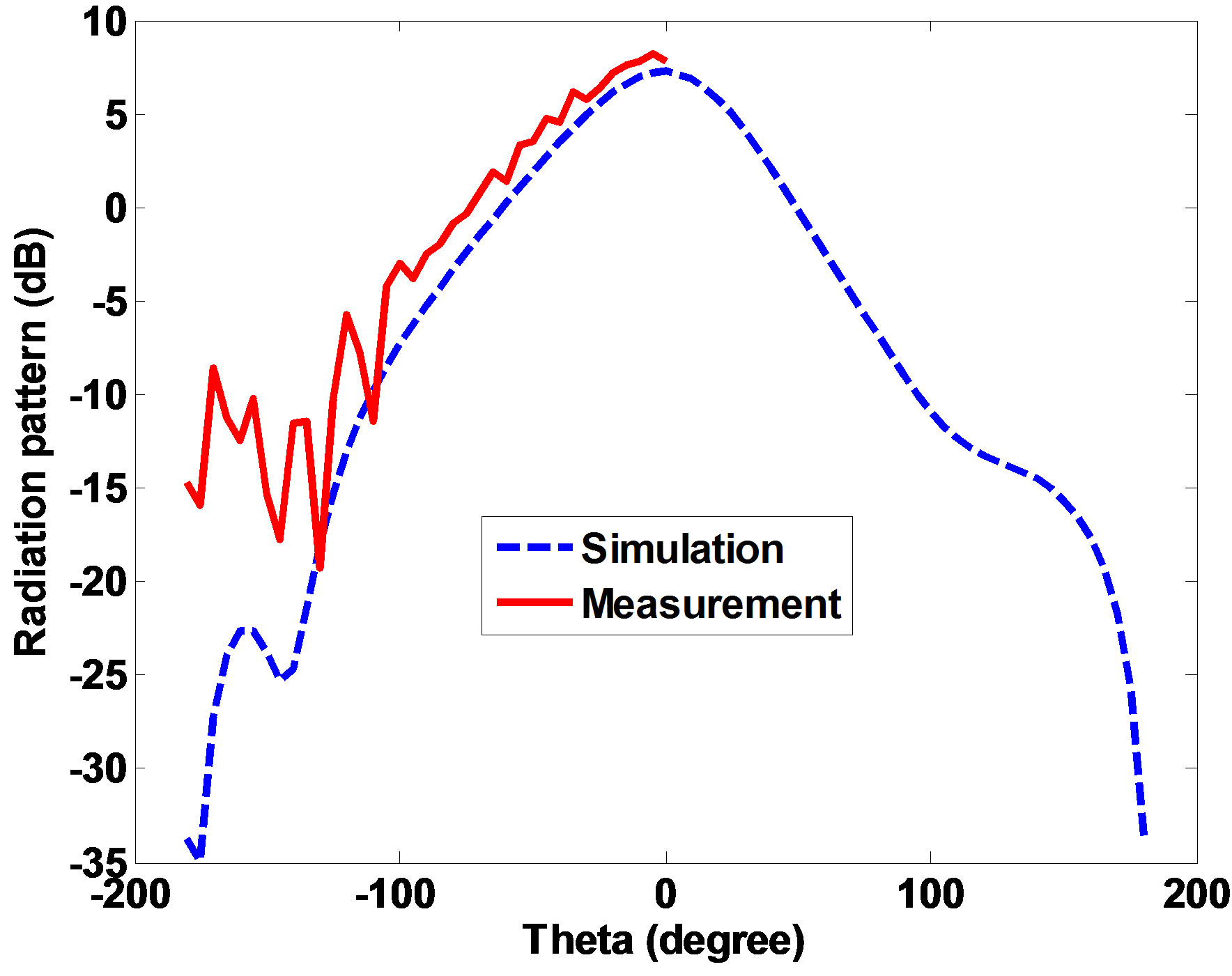
Finally, reasonable agreements between the simulated and measured radiation patterns in both the x-z and y-z planes are observed, as shown in Figure 12. The measured patterns away from the broadside in the x-z plane show some discrepancy, probably due to measurement uncertainties. The measured co-polarized and cross-polarized radiation patterns at 61 GHz are compared in Figure 13. One thing to notice is that the broadside gains in the y-z and x-z planes are different by about 1.4 dB. This discrepancy is also believed to be caused by experimental uncertainties.
5. Conclusion
A fully packaged left-hand circularly polarized antenna for 60 GHz wireless communications is demonstrated. Wide bandwidth and high efficiency are achieved by utilizing an air cavity and a fused-silica superstrate. The antenna packaging with a CPW interface is compatible to semiconductor integrated circuits. The measured antenna properties including return loss, axial ratio, gain and radiation patterns agree reasonably well with the simulation results. The demonstrated antenna achieved an impedance bandwidth greater 26%, a 6 dB axial ratio
 (a)
(a)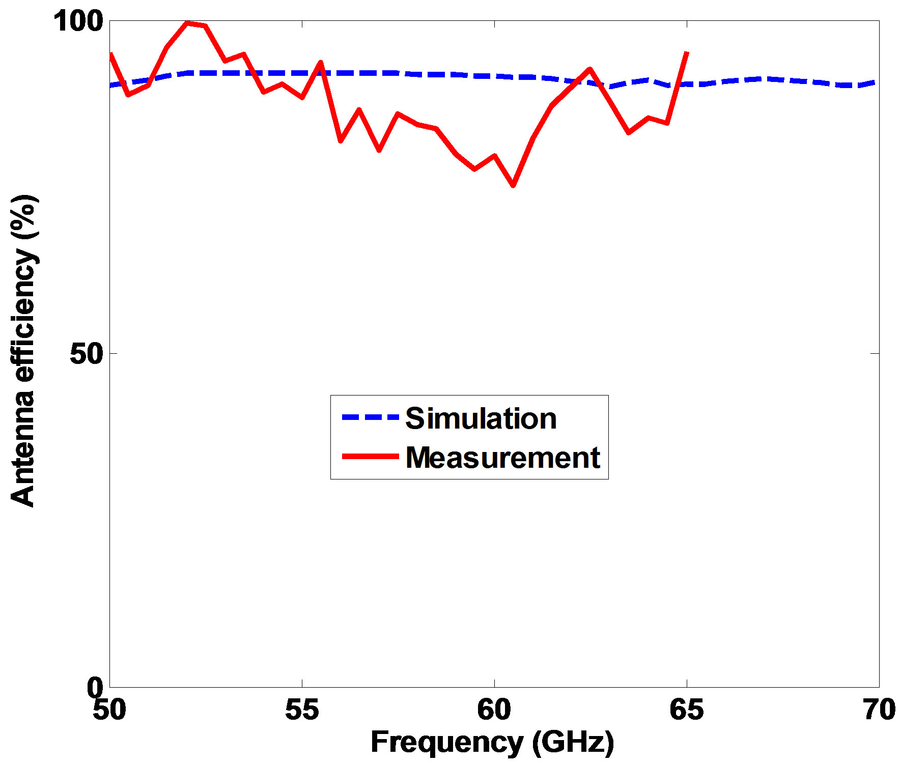 (b)
(b)
Figure 11. The simulated and measured antenna gain (a) and antenna efficiency (b) of the fully packaged antenna.
 (a)
(a)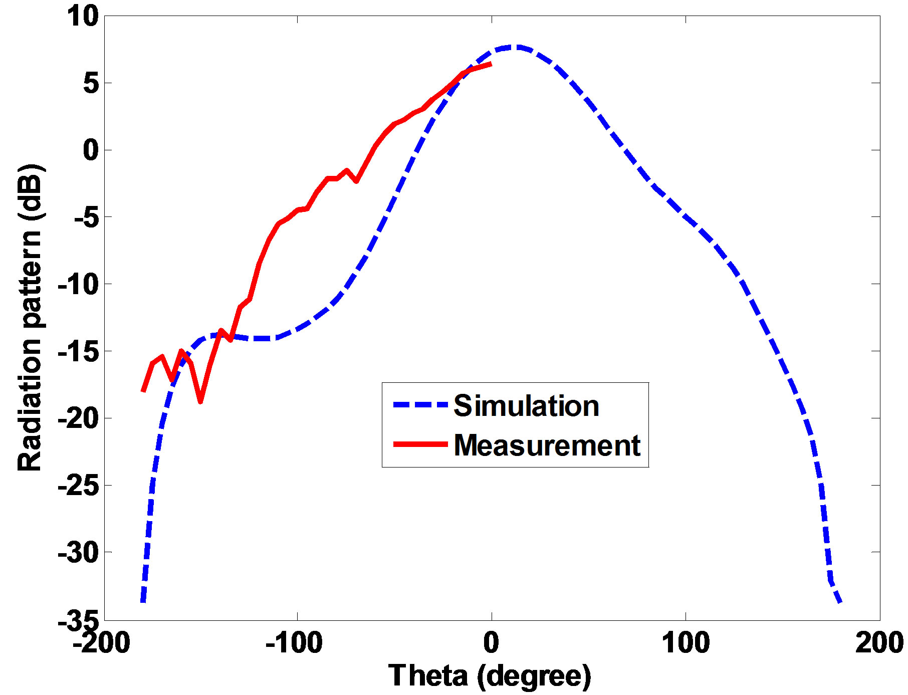 (b)
(b)
Figure 12. The simulated and measured radiation patterns of the fully packaged antenna at 61 GHz in: (a) y-z plane; (b) x-z plane.
 (a)
(a)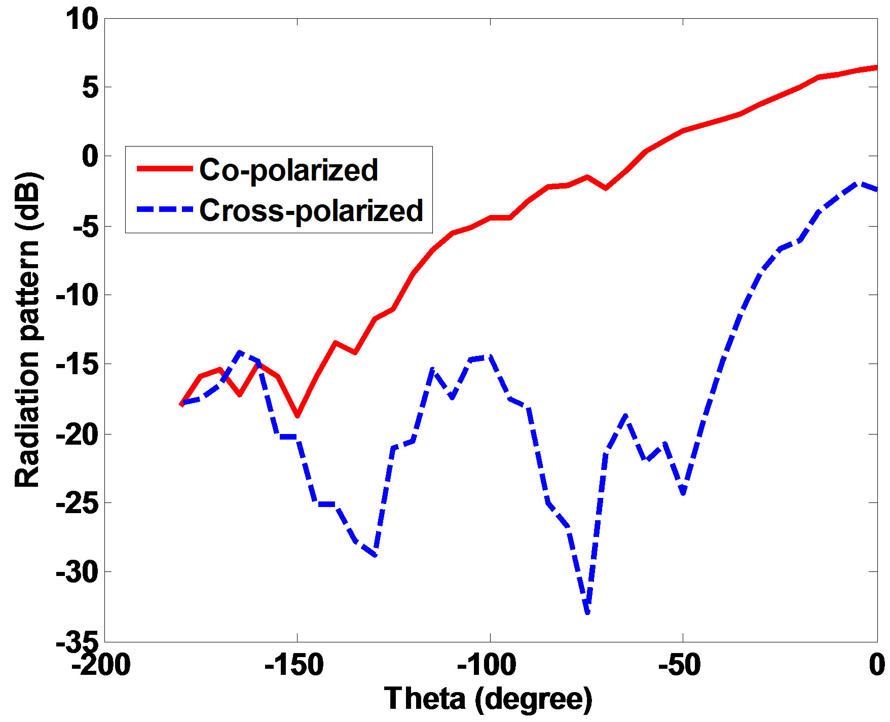 (b)
(b)
Figure 13. The measured co-polarized and cross-polarized radiation patterns of the fully packaged antenna at 61 GHz in: (a) y-z plane; (b) x-z plane.
bandwidth of 22.7% and efficiency above 75% for the entire frequency range.
6. Acknowledgements
This work was supported in part by the US Army Research Laboratory and by the US Army Research Office under agreement number W911NF-1-01-0285.
REFERENCES
- J. F. Buckwalter, et al., “An Integrated Subharmonic Coupled-Oscillator Scheme for a 60 GHz Phased-Array Transmitter,” IEEE Transaction on Microwave Theory Technology, Vol. 54, No. 12, 2006, pp. 4271-4280. doi:10.1109/TMTT.2006.885581
- T. S. Rappaport and D. A. Hawbaker, “Wide-Band Microwave Propagation Parameters Using Circular and Linear Polarized Antennas for Indoor Wireless Channels,” IEEE Transaction on Communication, Vol. 40, No. 2, 1992, pp. 240-245. doi:10.1109/26.129185
- T. Manabe, et al., “Polarization Dependence of Multipath Propagation and High-Speed Transmission Characteristics of Indoor Millimeter-Wave Channel at 60 GHz,” IEEE Transaction on Vehicle Technology, Vol. 44, No. 2, 1995, pp. 268-274. doi:10.1109/25.385918
- C. Loyez, N. Rolland, P. A. Rolland and O. Lafond, “Indoor 60 GHz Radio Channel Sounding and Related T/R Module Considerations for High Data Rate Communications,” Electronics Letter, Vol. 37, No. 10, 2001, pp. 654- 655. doi:10.1049/el:20010439
- M. Lye, R. B. Waterhouse, D. Novak, F. Zavosh and J. T. Aberle, “Design and Development of Printed Antenna Remote Units for Optically Distributed Mobile Communications,” IEEE Microwave Guided Wave Letter, Vol. 8, No. 12, 1998, pp. 432-434. doi:10.1109/75.746766
- N. C. Karmakar, “Investigations into a Cavity-Backed Circular-Patch Antenna,” IEEE Transaction on Antennas and Propagation, Vol. 50, No. 12, 2002, pp. 1706-1715. doi:10.1109/TAP.2002.807427
- N. Herscovici, “A Wide-Band Single-Layer Patch Antenna,” IEEE Transaction on Antennas and Propagation, Vol. 46, No. 4, 1998, pp. 471-474. doi:10.1109/8.664109
- M. M. Faiz and P. F. Wahid, “A High Efficiency L-Band Microstrip Antenna,” Proceeding on IEEE International URSI Conference, Orlando, 11-16 July 1999, pp. 272- 275.
- W. Choi, C. Pyo, Y. H. Cho, J. Choi and J. Chae, “High Gain and Broadband Microstrip Patch Antenna Using a Superstrate Layer,” IEEE Antennas and Propagation Society International Symposium Digest, Columbus, Vol. 2, 22-25 June 2003, pp. 292-295.
- L. Bernard, R. Loison, R. Gillard and T. Lucidarme, “High Directivity Multiple Superstrate Antennas with Improved Bandwidth,” IEEE Antennas and Propagation Society International Symposium Digest, San Antonio, Vol. 2, 16-21 June 2002, pp. 522-525.
- N. G. Alexopoulos and D. R. Jackson, “Fundamental Superstrate (Cover) Effects on Printed Circuit Antennas,” IEEE Transaction on Antennas and Propagation, Vol. 32, No. 8, 1984, pp. 807-816. doi:10.1109/TAP.1984.1143433
- J. Lee, N. Kidera, G. DeJean, S. Pinel, J. Laskar and M. M. Tentzeris, “A V-Band Front-End with 3-D Integrated Cavity Filters/Duplexers and Antenna in LTCC Technologies,” IEEE Transaction on Microwave Theory Technology, Vol. 54, No. 7, 2006, pp. 2925-2936. doi:10.1109/TMTT.2006.877440
- X. Tang, S. Xiao, B. Wang and J. Wang, “A 60 GHz Wideband Slot Antenna Based on Substrate Integrated Waveguide Cavity,” International Journal of Infrared and Millimeter Waves, Vol. 8, No. 4, 2007, pp. 275-281. doi:10.1007/s10762-007-9206-z
- M. Sun, Y. P. Zhang, K. M. Chua, L. L. Wai, D. Liu and B. P. Gaucher, “Integration of Yagi Antenna in LTCC Package for Differential 60 GHz Radio,” IEEE Transaction on Antennas and Propagation, Vol. 56, No. 8, 2008, pp. 2780-2783. doi:10.1109/TAP.2008.927577
- S. Hu, Y. Xiong, L. Wang, R. Li and T. Lim, “A Millimeter-Wave Wideband High-Gain Antenna and Its 3D System-in-Package Solution in a TSV-Compatible Technology,” Electronic Components and Technology Conference, Lake Buena Vista, 31 May-3 June 2011, pp. 869- 872.
- S. Hu, Y. Xiong, L. Wang, R. Li, J. Shi and T. Lim, “Compact High-Gain mmWave Antenna for TSV-Based System-in-Package Application,” IEEE Transactions on Components, Packaging and Manufacturing Technology, Vol. 2, No. 5, 2012, pp. 841-846. doi:10.1109/TCPMT.2012.2188293
- R. Sauleau and P. Coquet, “Input Impedance of Electromagnetic Bandgap Resonator Antennas,” Microwave and Optical Technology Letter, Vol. 41, No. 5, 2004, pp. 369- 375. doi:10.1002/mop.20144
- S. J. Franson and R. W. Ziolkowski, “Gigabit per Second Data Transfer in High-Gain Metamaterial Structures at 60 GHz,” IEEE Transaction on Antennas and Propagation, Vol. 57, No. 10, 2009, pp. 2913-2925. doi:10.1109/TAP.2009.2029277
- A. E. I. Lamminen, A. R. Vimpari and J. Säily, “UC-EBG on LTCC for 60-GHz Frequency Band Antenna Applications,” IEEE Transaction on Antennas and Propagation, Vol. 57, No. 10, 2009, pp. 2904-2912. doi:10.1109/TAP.2009.2029311
- I. Khromova, R. Gonzalo, I. Ederra, J. Teniente, K. Esselle and P. De-Hon, “Novel All-Dielectric mmWave Horn Antennas Based on EBG Structures,” Proceedings of the 5th European Conference on Antenna and Propagation, Rome, 11-15 April 2011, pp. 2959-2961.
- A.-C. Bunea, F. Craciunoiu and G Sajin, “28 GHz CRLH Antenna on Silicon Substrate,” Proceedings of the 41st European Microwave Conference, Manchester, 10-13 October 2011, pp. 579-582.
- G. M. Rebeiz, “Millimeter-Wave and Terahertz Integrated Circuit Antennas,” Proceedings of the IEEE, Vol. 80, No. 11, 1992, pp. 1748-1770. doi:10.1109/5.175253
- D. Nesic, A. Nesic and V. Brankovic, “Circular Polarised Printed Antenna Array with Broadband Axial Ratio,” IEEE Antennas and Propagation Society International Symposium Digest, Columbus, 22-25 June 2003, pp. 912- 915.
- K. Kim, S. Pinel, S. Laskar and J. Yook, “Circularly & Linearly Polarized Fan Beam Patch Antenna Arrays on Liquid Crystal Polymer Substrate for V-Band Applications,” Asia Pacific Microwave Conference proceedings, Suzhou, 4-7 December 2005.
- H. Uchimura, N. Shino and K. Miyazato, “Novel Circular Polarized Antenna Array Substrates for 60 GHz-Band,” IEEE MTT-S International Microwave Symposium Digest, Long Beach, 14-18 June 2005, pp. 1875-1878. doi:10.1109/MWSYM.2005.1517099
- M. Barakat, C. Delaveaud and F. Ndagijimana, “Circularly Polarized Antenna on SOI for the 60 GHz Band,” Proceedings of the 2nd European Conference on Antenna and Propagation, Edinburgh, 11-16 November 2007, pp. 1-6.
- R. Zhou, D. Liu and H. Xin, “Design of Circularly Polarized Antenna for 60 GHz Wireless Communications,” Proceedings of the 3rd European Conference on Antenna and Propagation, Berlin, 23-27 March 2009, pp. 3787- 3789.
- J. Balcells, Y. Damgaci, B. A. Cetiner, J. Romeu and L. Jofre, “Polarization Reconfigurable MEMS-CPW Antenna for mmWave Applications,” Proceedings of the 4th European Conference on Antenna and Propagation, Barcelona, 12-16 April 2010, pp. 1-5.
- T. Zwick, C. Baks, U. Pfeiffer, D. Liu and B. Gaucher, “Probe Based MMW Antenna Measurement Setup,” IEEE Antennas and Propagation Society International Symposium Digest, Monterey, 20-26 June 2004, pp. 747- 750.
- U. R. Pfeiffer, et al., “A Chip-Scale Packaging Technology for 60 GHz Wireless Chipsets,” IEEE Transaction on Microwave Theory Technology, Vol. 54, No. 8, 2006, pp. 3387-3397. doi:10.1109/TMTT.2006.877832
- J. Grzyb, D. Liu, U. Pfeiffer and B. Gaucher, “Wideband Cavity-Backed Folded Dipole Superstrate Antenna for 60 GHz Applications,” IEEE Antennas and Propagation Society International Symposium Digest, 5-10 June 2006, pp. 3939-3942.
- P. C. Sharma and K. C. Gupta, “Analysis and Optimized Design of Single Feed Circularly Polarized Microstrip Antennas,” IEEE Transaction on Antennas and Propagation, Vol. 31, No. 6, 1983, pp. 949-955. doi:10.1109/TAP.1983.1143162
- J. L. Kerr, “Microstrip Polarization Techniques,” Proceeding of Antenna Applications Symposium, 20-22 September 1978, 19 p.
- C. A. Balanis, “Antenna Theory, Analysis and Design,” 1st Edition, John Wiley & Sons, New York, 1982.
- J. P. Raskin, G. Gauthier, L. P. B. Katehi and G. M. Rebeiz, “Mode Conversion at GCPW-to-Micros-Trip-Line Transition,” IEEE Transaction on Microwave Theory Technology, Vol. 48, No. 1, 2000, pp. 158-161. doi:10.1109/22.817486