Soft Nanoscience Letters
Vol.1 No.3(2011), Article ID:6168,6 pages DOI:10.4236/snl.2011.13010
Size-Tunable Porous Anodic Alumina Nano-Structure for Biosensing
![]()
1Electrical Engineering Division, Department of Engineering, University of Cambridge, Cambridge, UK; 2Brunel Institute for Bioengineering, Brunel University, Uxbridge, Middlesex, UK; 3Department of information Display, Kyung Hee University, Seoul, South Korea.
E-mail: zhigang.zhu259@gmail.com
Received May 20th, 2011; revised June 18th, 2011; accepted June 24th, 2011.
Keywords: Porous Anodic Alumina, Anodization Electropolishing, Pore-Size, Electrode Array.
ABSTRACT
A porous anodic alumina (PAA) film has been investigated to realise highly-ordered nano-porous structures. A two-step anodization process is used to anodize aluminium into size-controllable aluminium oxide. In this paper, we investigate how anodization parameters affect nano-porous structures, such as voltage and time of pretreatment, anodization voltage and time, pore widening time. The results showed pretreatment is important to obtain a smooth surface for anodizing. The pore size is controllable between 30 and 80 nm, with a linear fit curve. The interpore size is constant at around 95 nm, and the pore densities are between 1010 and 1011 cm–2. The formation of straight vertical walls is crucial if the PAA film is to be subsequently used as the template for the growth of metal nanowire arrays.
1. Introduction
Porous anodic alumina (PAA) film was discovered by Masuda and Fukuda in 1995, who developed a two-step replicating process to achieve a uniform, closely packed honeycomb structure [1]. Since then, PAA films have been widely used as a template for the growth of nanostructured materials and devices, and provide an ideal route to fabricate nanowires or nanotube arrays [2], including carbon nanotubes [3], silicon [4], metal [5], semiconductors [6] and polymers [7]. The PAA film also has wide range of potential applications in microand nano-electronics, photoelelctronics, information storage and lithium ion batteries [2]. There is also particular relevance to the biosensors as the high surface to volume ration can lead to improve sensitivity, detection limit, signal to noise ratio and electron-transfer ratio compared to conventional electrodes [8]. The natural sub-micron scale nanostructure of PAA overcomes the limit of traditional lithography techniques on the nano-scale. For example, it provides fundamental nano-metre scale porosity, as the pore diameter and inter-pore distance sizes are controllable. Nevertheless, a high aspect ratio can be easily achieved to enable the growth of nanowires and chemically and thermally stability can benefit for future application [9].
Template-assisted electrodeposition through a PAA film has been shown to be a cost-effective and high yield fabrication technique for producing nanowire arrays, and thus highly ordered hexagonal arrays of parallel metallic nanowires (Cu, Ni, Au) can be synthesized by electrodeposition [10]. Platinum is a frequently used noble metal in the field of biosensors and Pt nano-wires are widely used to immobilize enzymes for the fabrication of biosensors [11-13]. To achieve highly ordered Pt nano-wire arrays through PAA templates, the size and thickness of PAA films should be tuneable and controllable.
In this work, a PAA template was fabricated by twostep anodization in 0.3 M oxalic acid. The objective of this study is to optimise the fabrication of PAA films, which have controllable thickness and highly-ordered uniform pore size. We found that electropolishing (EP) prior to anodization plays an important role in smoothing the surface and thus leads to the growth of ordered nanopore structures. The effect of time and voltage on EP was investigated to optimise the best condition. Furthermore, anodizing time and voltage, and pore widening time were thoroughly studied to achieve regular and controllable PAA films.
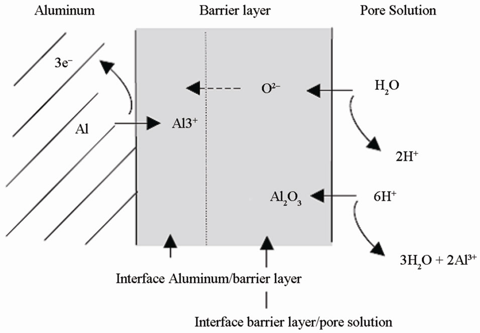
Figure 1. Interface formation during the anodization process.
2. Experimental
2.1. Working Mechanism
The formation of porous oxide layer involves two major chemical reactions: the formation of alumina and the dissolution of alumina. The rates of these two chemical reactions are equivalent so that pores are formed, as shown in Figure 1.
Aluminum oxide is formed at the anode through the reaction:
 (1)
(1)
Aluminum oxide dissolution takes place at the cathode:
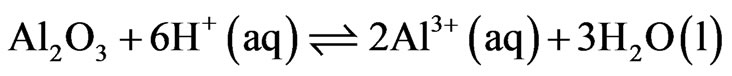 (2)
(2)
When the circuit is completed, an electric field is being produced. The surface of aluminum metal is not ideally smooth; cracks and film roughness result in localized surface curvature. The electric field will be enhanced at regions of the surface where there is high local surface curvature. The pores grow and increase their depth with anodizing time.
In order to get self-ordered nano-pore arrays, a twostep anodization is employed. A highly pure aluminum foil was first anodized for 6 hours in 0.3 M oxalic acid at 40 V and 2˚C. However, less self-ordered and less regular pore size of nano-hole arrays could be obtained from this first porous oxide layer. Therefore, the first oxide layer is eliminated by acid etching. Etching allows the metal layer to come out, and consists of self-ordered and regular pore basement. We can then introduce a second anodization process base on this more regular metal template. As a result, highly self-ordered nano-hole arrays can be produced [5].
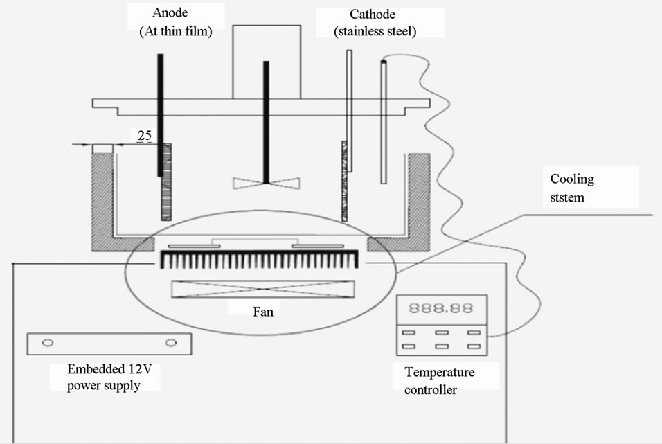
Figure 2. Experimental setup for anodizing PAA film.
2.2. Pretreatment of Al foil
Highly pure aluminium foils (250 µm in thickness, 99.99%, Goodfellow, UK) were pre-treated to clean the surface and reduce intrinsic stress. The aluminium foil was cut into 0.3 × 2.5 cm pieces. All the foil samples were immersed in acetone for degreasing for 1 hour. Then, the foils were washed in an ultrasonic bath for 2 minutes. Afterwards, the foils were immersed in 3.0 M NaOH for 2 minutes for alkaline etching. Finally, the foils were electropolished for different times in perchloride acid at 20 V and 0˚C
2.3. Anodization Process
The experimental setup is illustrated in Figure 2. The foil was first anodized in 0.3 M oxalic acid for 6 hours at 40 V and 2˚C. After the first anodization, the foil was immersed in Cr2O5/H3PO4 acid for 1 hour for etching. Afterwards, the foil was anodized for a second time under different conditions; it is for this step that the effect of the anodization upon the pore structure is studied.
2.4. Characterization
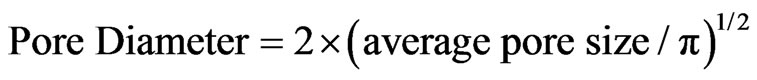
The foil samples were studied using several analysis techniques. A Zeiss Supra 35VP (Germany) Field Emission Scanning Electron Microscope (FESEM) in second electron mode was used to observe the nano-structure of pores and its cross section. Energy Dispersive X-ray was used to investigate the elemental compositions in the sample. A Digital Instruments Nanoscope III (USA) Atomic Force Microscope (AFM) in tapping mode was used to observe the surface morphologies of the sample.
In addition, ImageJ software was used to measure pore diameter to obtain average pore area and pore density from
 (3)
(3)
 (a)
(a)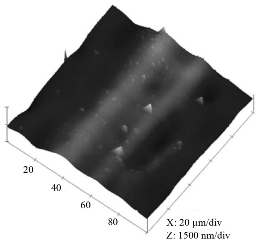 (b)
(b)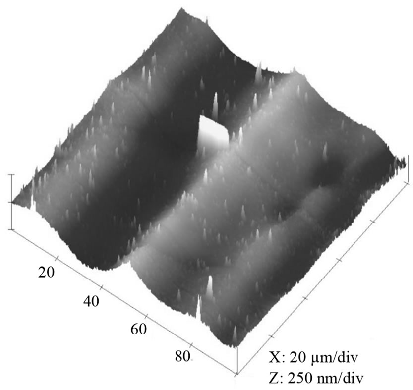 (c)
(c)
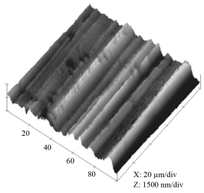
Figure 3. Effect of electropolishing time for a) 0 s; b) 40 s; c) 120 s on the surface morphology of Al film at 20 V in a mixture of perchloric acid and ethanol (1:4 v/v). The mean roughness’s (Ra) are 0.28 µm, 0.20 µm and 0.05 µm, respectively; the maximum vertical distances (Rt) are 1.53 µm, 1.1 µm and 0.23 µm, respectively.
 (4)
(4)
3. Results and Discussion
The surface condition of the Al foil has a great influence on the formation of nano-structured alumina, and thus electropolishing was chosen to minimise the surface defects and obtain a smoother working surface. Figure 3 indicates that electropolishing has a large effect on the surface morphology of the Al film. The as-cleaned sample (Figure 3(a), without EP) shows a rough surface with maximum vertical distance (Rt) 1.53 µm, while the mean roughness (Ra) is 0.28 µm. After electropolishing for 40 s (Figure 3(b)), the maximum vertical distance reduces to 1.11 µm, whist the Ra decreases to 0.20 µm. Figure 3(c) indicates that Rt could be further reduced to 0.23 µm as the EP time was extended to 120 s. Therefore, the maximum vertical distance revealed that the roughness of the sample electropolished for 120 s was the smallest while the raw material one showed the largest value. However, more holes will occur on the surface if EP time was prolonged to 180 s or more. Therefore, the foil, electropolished for 120 s, contained greatest smoothness and this was used in future experiments.
Our investigation showed that the time for second anodization would not affect the pore diameter and interpore size. And it is believed that anodizing time affected mostly on the thickness of oxide layer rather than pore diameter. Figure 4 proves our suggestion and indicates that the aluminium oxide layer thickness is controllable.
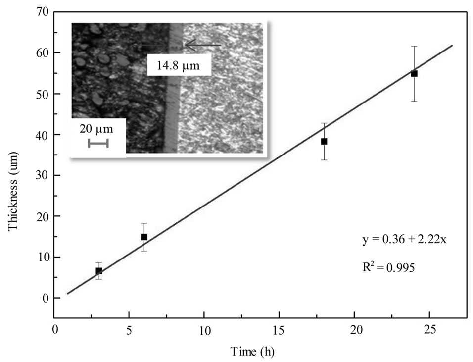
Figure 4. Effect of anodizing time on the thickness of aluminium oxide layer, the insert is the PAA film mounted in a resin and observed in microscope.
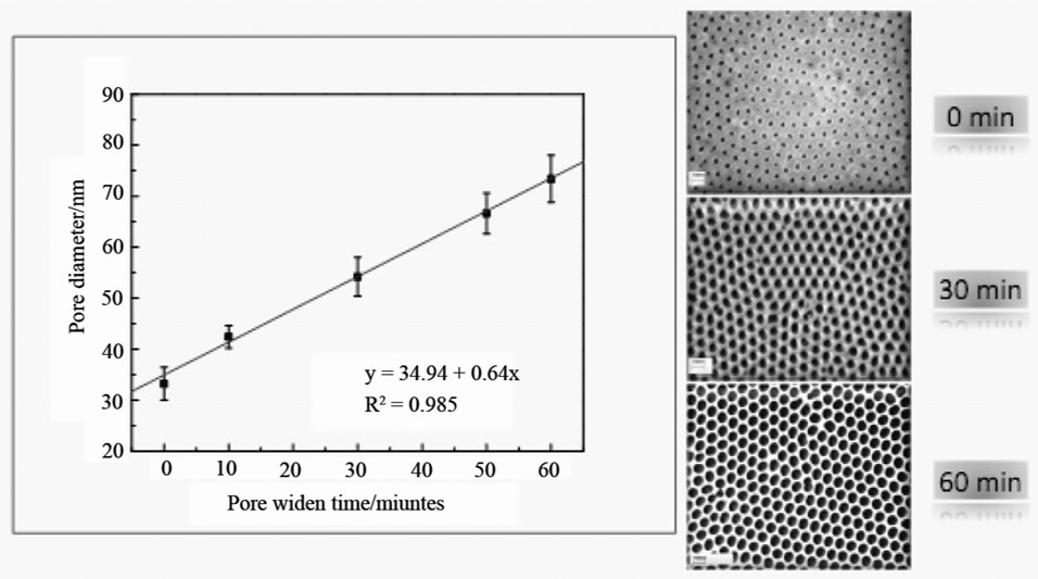
Figure 5. Effect of pore widening time on the pore sizes, the SEM images show the samples anodised in 0, 30 and 60 minutes, respectively.
The thickness of the porous oxide layer will increase in second anodizing time, and the thickness of samples anodised at different times is shown in the Figure 4. A linear fit can be achieved by plotting the thickness (µm) of the oxide layer against the second anodizing time (h), with y (µm) = 0.36 + 2.22x (s). This linear relationship is very important for synthesis of nano-electrode arrays with different aspect ratios. Cu nano-rods only require a small aspect ratio, while carbon nano-tube arrays need ultra-high aspect ratios (1000:1).
It was reported that the anodization voltage, as well as electrolyte, concentration and temperature have major effects on both pore diameter and interpore size [14]. The pore diameter developed here is 35 nm and the interpore size is 95 nm. Li, et al. reported that volume expansion of the aluminium turning into alumina during oxidization plays an important role and a moderate expansion value (1.4) is most suitable for self-organized formation in PAA films [15]. The calculated value of vo-
 (a)
(a)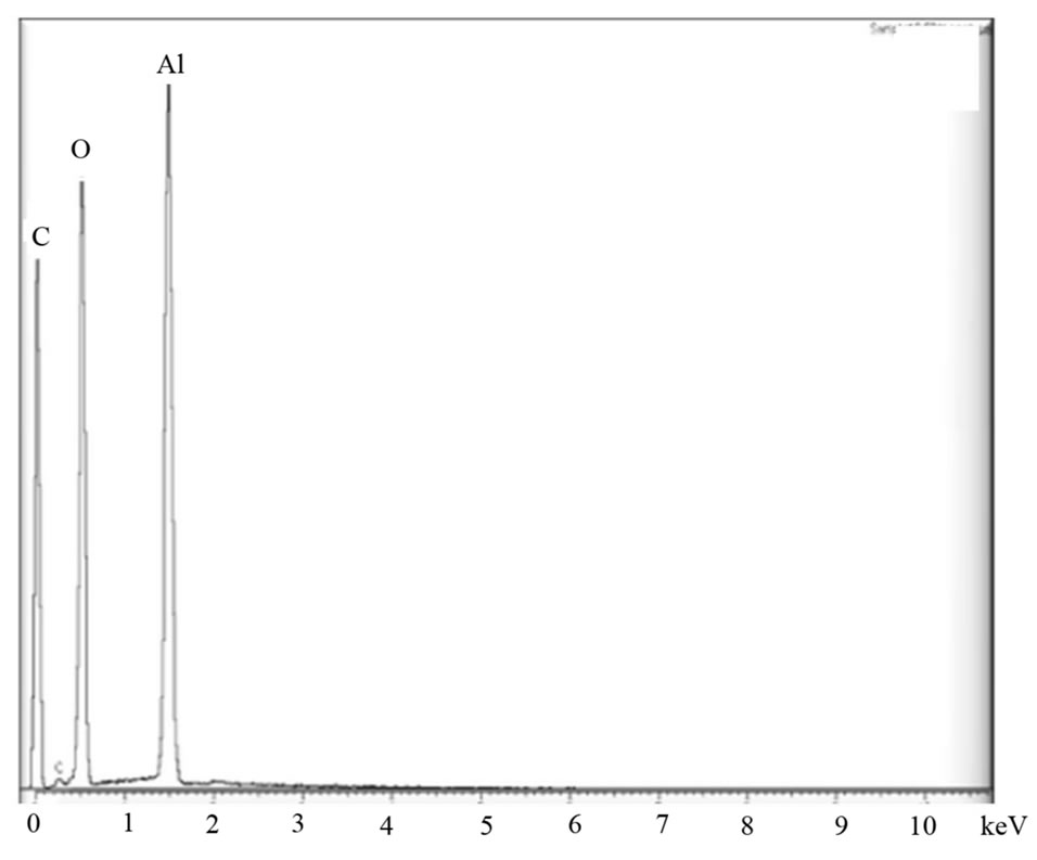 (b)
(b)
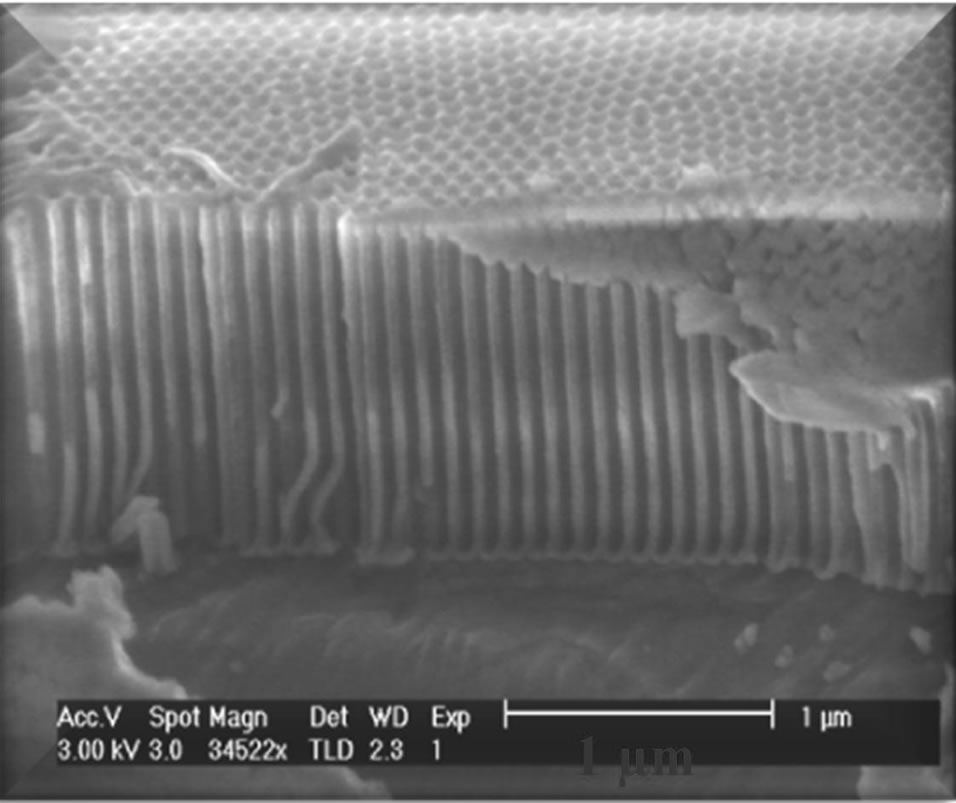
Figure 6. (a) SEM image of cross section in a PAA film, (b) EDX analysis illustrates that only Al and O elements were found in the film.
lume expansion (Al2O3:Al) in our samples is 1.46, which is thus very close to the value suggested by Li, et al. to fabricate the highly-ordered PAA films.
The influence of the anodic voltage (20, 30, 40 and 60 V respectively) on the porosity of the PAA film has also been studied. There was no obvious trend when the anodizing voltage increased. This might be due to the conditions applied in the first anodization step. During the first anodization, Al foils were anodized at 40 V and 2˚C in 0.3 M oxalic acid and then the second anodization process follows. Pores are already formed during the first anodization. These pores had their size fixed by the 40 V anodic voltage. Therefore, we obtained similar results though different anodizing voltage applied in the second anodization.
The ability to control pore diameter of PAA films would facilitate device design in the future. The sizes of pore changes with the immersion time in 5 wt% H3PO4, as showed in Figure 5. According to the SEM images and the analysis of ImageJ software, the size of the pores of the PAA film can be calculated. The raw film shows the size is 33 nm, and it can increase to 54 nm after immersion for 30 mins, and further increase to 73.4 nm after pore-widening for 60 mins. The linear curve can be achieved by plotting the pore distance to pore widening time, with y (µm) = 34.94 + 0.64x (s). The interpore size is around 95 nm, and is independent on the pore-widening time. The pore densities are between 1010 and 1011 cm–2. It was believed that the widening of the pore by the phosphoric acid was too fast and that all the pores merged together after 3 hours of immersion time. Therefore, no more edges or boundaries could be observed.
Figure 6 shows that straight vertical walls, from top to bottom, were formed during the anodization process. This straight characteristic is crucial in order to facilitate the growth of CNTs or metal nanowire arrays in the next electrodeposition process. Energy dispersive X-ray spectroscopy (EDX) analysis indicates that only two elements can be observed. There are Al and O, while the occurrence of the C element is due to the signal from Carbon conductive tapes. EDX analysis is able to confirm that all the aluminium is oxidized to alumina.
4. Conclusions
Highly ordered porous anodic alumina films have been fabricated by a two-step anodizing method. Pretreatment plays an important role and electropolishing for 120 s yields the smoothest surface. The size and porosity of the film is controllable, with thickness various between 5 and 100 µm and pore size between 30 and 80 nm. The interpore size is around 95 nm, and is independent of the immersion time. The pore densities are about 1010 - 1011 cm–2. Also straight vertical walls were formed during the anodizing process, which will facilitate the growth of CNT or metal nanowire arrays in the next steps.
5. Acknowledgements
This research was supported by the Royal Society grant (RG 2009/R1), the National Institute of Health (NIH/ NIBIB) grant (R01EB001640) and the grant from EU Framework Programme 7 (CORONA, CP-FP 213969-2). We would like to thank Miss. Cheung Hoi Ki who was involved this work as part of her Internship Programme as an Exchange Student.
REFERENCES
- H. Masuda and K. Fukuda, “Ordered Metal Nanohole Arrays Made by a 2-Step Replication of Honeycomb Structure of Anodic Alumina,” Science, Vol. 268, No. 5216, 1995, pp. 1466-1468. doi:10.1126/science.268.5216.1466
- Y. Z. Piao and H. Kim, “Fabrication of Nanostructured Materials Using Porous Alumina Template and Their Applications for Sensing and Electrocatalysis,” Journal of Nanoscience and Nanotechnology, Vol. 9, No. 4, 2009, pp. 2215-2233. doi:10.1166/jnn.2009.SE42
- G. P. Sklar, K. Paramguru, M. Misra and J. C. LaCombe, “Pulsed Electrodeposition into AAO Templates for CVD Growth of Carbon Nanotube Arrays,” Nanotechnology, Vol. 16, No. 8, 2005, pp. 1265-1271. doi:10.1166/jnn.2009.SE42
- B. S. Chen, Q. L. Xu, X. L. Zhao, X. G. Zhu, M. G. Kong and G. W. Meng, “Branched Silicon Nanotubes and Metal Nanowires via AAO-Template-Assistant Approach,” Advanced Functional Materials, Vol. 20, No. 21, 2010, pp. 3791-3796. doi:10.1166/jnn.2009.SE42
- T. Yanagishita, K. Nishio and H. Masuda, “Fabrication of Metal Nanohole Arrays with High Aspect Ratios Using Two-Step Replication of Anodic Porous Alumina,” Advanced Materials, Vol. 17, No. 18, 2005, pp. 2241-2243. doi:10.1166/jnn.2009.SE42
- F. M. Han, G. W. Meng, X. L. Zhao, Q. L. Xu, J. X. Liu, B. S. Chen, X. G. Zhu and M. G. Kong, “Building Desired Heterojunctions of Semiconductor CdS Nanowire and Carbon Nanotube via AAO Template-Based Approach,” Materials Letters, Vol. 63, No. 26, 2009, pp. 2249-2252. doi:10.1016/j.matlet.2009.07.044
- A. Drury, S. Chaure, M. Kroell, V. Nicolosi, N. Chaure and W. J. Blau, “Fabrication and Characterization of Silver/Polyaniline Composite Nanowires in Porous Anodic Alumina,” Chemistry of Materials, Vol. 19, No. 17, 2007, pp. 4252-4258. doi:10.1021/cm071102s
- H. B. Shi and J. I. Yeh, “Part I: Recent Developments in Nanoelectrodes for Biological Measurements,” Nanomedicine, Vol. 2, No. 5, 2007, pp. 587-598. doi:10.2217/17435889.2.5.587
- A. S. M. Chong, L. K. Tan, J. Deng and H. Gao, “Soft Imprinting: Creating Highly Ordered Porous Anodic Alumina Templates on Substrates for Nanofabrication,” Advanced Functional Materials, Vol. 17, No. 10, 2007, pp. 1629-1635. doi:10.1002/adfm.200600993
- A. J. Yin, J. Li, W. Jian, A. J. Bennett and J. M. Xu, “Fabrication of Highly Ordered Metallic Nanowire Arrays by Electrodeposition,” Applied Physics Letters, Vol. 79, No. 7, 2001, pp. 1039-1041. doi:10.1063/1.1389765
- Y. S. Lu, M. H. Yang, F. L. Qu, G. L. Shen and R. Q. Yu, “Amperometric Biosensors Based on Platinum Nanowires,” Analytical Letters, Vol. 40, No. 5, 2007, pp. 875- 886. doi:10.1080/00032710701242071
- J. H. Yuan, K. Wang and X. H. Xia, “Highly Ordered Platinum-Nanotubule Arrays for Amperometric Glucose Sensing,” Advanced Functional Materials, Vol. 15, No. 5, 2005, pp. 803-809. doi:10.1002/adfm.200400321
- M. H. Yang, F. L. Qu, Y. S. Lu, Y. He, G. L. Shen and R. Q. Yu, “Platinum Nanowire Nanoelectrode Array for the Fabrication of Biosensors,” Biomaterials, Vol. 27, No. 35, 2006, pp. 5944-5950. doi:10.1016/j.biomaterials.2006.08.014
- M. S. Sander, A. L. Prieto, R. Gronsky, T. Sands and A. M. Stacy, “Fabrication of High-Density, High Aspect Ratio, Large-Area Bismuth Telluride Nanowire Arrays by Electrodeposition into Porous Anodic Alumina Templates,” Advanced Materials, Vol. 14, No. 9, 2002, pp. 665- 667. doi:10.1002/1521-4095(20020503)14:9<665::AID-ADMA665>3.0.CO;2-B
- A. P. Li, F. Muller, A. Birner, K. Nielsch and U. Gosele, “Hexagonal Pore Arrays with a 50 - 420 nm Interpore Distance Formed by Self-Organization in Anodic Alumina,” Journal of Applied Physics, Vol. 84, No. 11, 1998, pp. 6023-6026. doi:10.1063/1.368911