Graphene
Vol.04 No.03(2015), Article ID:58355,8 pages
10.4236/graphene.2015.43005
Localization of Charge Carriers in Monolayer Graphene Gradually Disordered by Ion Irradiation
Erez Zion1, Avner Haran2, Alexander V. Butenko1, Leonid Wolfson3, Yuri Kaganovskii3, Tal Havdala1, Amos Sharoni1, Doron Naveh2, Vladmir Richter4, Moshe Kaveh3, Eugene Kogan3, Issai Shlimak3*
1Department of Physics and Institute of Nanotechnology and Advanced Materials, Bar-Ilan University, Ramat-Gan, Israel
2Faculty of Engineering, Bar-Ilan University, Ramat-Gan, Israel
3Jack and Pearl Resnick Institute, Department of Physics, Bar-Ilan University, Ramat-Gan, Israel
4Solid State Institute and Physics Department, Technion-Israel Institute of Technology, Haifa, Israel
Email: *Issai.Shlimak@biu.ac.il
Copyright © 2015 by authors and Scientific Research Publishing Inc.
This work is licensed under the Creative Commons Attribution International License (CC BY).
http://creativecommons.org/licenses/by/4.0/


Received 16 June 2015; accepted 24 July 2015; published 28 July 2015
ABSTRACT
Gradual localization of charge carriers is studied in a series of micro-size samples of monolayer graphene fabricated on the common large scale film and irradiated by different doses of C+ ions with energy 35 keV. Measurements of the temperature dependence of conductivity and magnetoresistance in fields up to 4 T show that at low disorder, the samples are in the regime of weak localization and antilocalization. Further increase of disorder leads to strong localization regime, when conductivity is described by the variable-range-hopping (VRH) mechanism. A crossover from the Mott regime to the Efros-Shklovskii regime of VRH is observed with decreasing temperature. Theoretical analysis of conductivity in both regimes shows a remarkably good agreement with experimental data.
Keywords:
Graphene, Localization, Hopping Conductivity, Ion Irradiation

1. Introduction
Graphene, a sheet of sp2-bonded carbon atoms, for several years already continues to be in the focus of attention of physics community, due to its potentially transformative impact across a wide range of applications including advanced electronics and sensing. Carrier scattering in graphene can be due to all kinds of disorder, including ripples in the graphene layer, point defects and their associated short-range potentials, charged impurities residing in the supporting substrate, and adsorbed atoms on the surface. Investigation of the influence of disorder on the properties of graphene is attracting a tremendous interest due to possibility to modify this novel and promising material using weak or strong localization of charge carriers. By controllably introducing defects into graphene, one may be able to understand how these mechanisms limit transport.
Previously, there were observed separately either weak localization (WL) or different kinds of Variable- Range-Hopping (VRH) conductivity of strongly localized carriers in graphene samples disordered by different methods like doping, oxidation, ion irradiation (see, for example, [1] -[8] ). However, we are not aware of observations of all regimes of localization with gradual increase of disordering in graphene. In this paper we report the results of study of the localization process in monolayer graphene (MG) samples subjected by different doses of ion irradiation.
The initial large size (5 ´ 5 mm) specimens were supplied by “Graphenea” company. Monolayer graphene was produced by CVD on copper catalyst and transferred to a 300 nm SiO2/Si substrate using wet transfer process. It is specified in the certificate, that the sheet resistivity of the specimen is 350 Ohm/sq. On one specimen, gold electrical contacts were deposited directly on the graphene surface. This sample was marked as 0. The resistivity of the sample 0 was 380 Ohm/sq which was close to the data in the certificate. On the surface of the other specimen, six groups of mini-samples (200 ´ 200 μm) were fabricated by means of electron-beam lithography (EBL) as well as electrical contacts (5 nm Ti and 45 nm Pd) for 2-probe measurements. The samples from the first group, marked as sample 1 were not irradiated, while 5 other groups were subjected to different doses (from  up to
up to  cm−2) of irradiation by C+ ions with energy 35 keV. Ion irradiation was performed on HVEE-350 Implanter, C+ ions were obtained from the hollow cathode ion source by CO2 decomposition.
The choice of the irradiation conditions is not occasional. They are the same as in [6] where the Hall Effect was measured in monolayer graphene subjected to ion irradiation. Resistances of the initial sample as in [6] and our initial sample 0 are the same. It is shown in [6] that both Hall coefficient and mobility are temperature independent up to high dose of irradiation. Moreover, it is shown that the sheet Hall concentration of charge carriers (about 1013 cm−2) does not depend on the dose of irradiation at all. We are based on these results in our decision to prefer the 2-probe geometry instead of the Hall bar geometry, because this allows us to measure more samples on the same sample holder. As a result, we are able to enhance the reproducibility of the obtained results. Comparison of the graphene resistance measured by 2-probe method and by 4-probe method presented in [6] shows that in this system, contact resistance is insignificant.
In our previous work [9] , a concentration of structural defects ND was determined for each group of samples using measurements of the Raman scattering. These values are shown in the inset in Figure 1 (it turns out that sample 1 is also slightly disordered due to EBL process). Measurements of the current-voltage characteristics (I-V) for all samples, performed at room temperature, show that for samples 5 and 6, I-V is strongly non-linear even at very small current. That is why in this paper, the temperature dependences of resistance R(T) are shown only for samples 0 - 4.
The resistance is measured by two-probe method in helium cryostat down to 1.8 K in zero magnetic fields and in magnetic fields up to 4 Tesla. Figure 1 shows the general picture R(T) for all samples. The sample 0 shows typical metallic behavior, when R slightly decreases with decrease of T. For sample 1, R slightly increases with decreasing T, which is characteristic for “dirty” metals. For other samples R changes with T exponentially, which is characteristic for strongly localized carriers.
2. Weak Localization
Figure 2 shows the experimental dependences of magnetoconductance (MC) of sample 1 in wide temperature interval, from 300 K down to 1.8 K. Plot of the temperature dependence of conductivity on the scale  vs. ln T (Figure 3) shows the logarithmic temperature behavior of
  at low T, characteristic for regime of WL [10] , with tendency to saturation at very low temperatures.
WL regime of conductivity in monolayer graphene has important features due to the facts that charge carriers are chiral Dirac fermions, which are reside in two inequivalent valleys at the K and K' points of the Brillouin zone. Due to chirality, Dirac fermion acquires a phase of  upon intravalley scattering, which leads to destructive interference with its time-reversed counterpart and weak antilocalization (WAL). Intervalley scattering leads to restoration of WL because fermions in K and K' valleys have opposite chiralities.
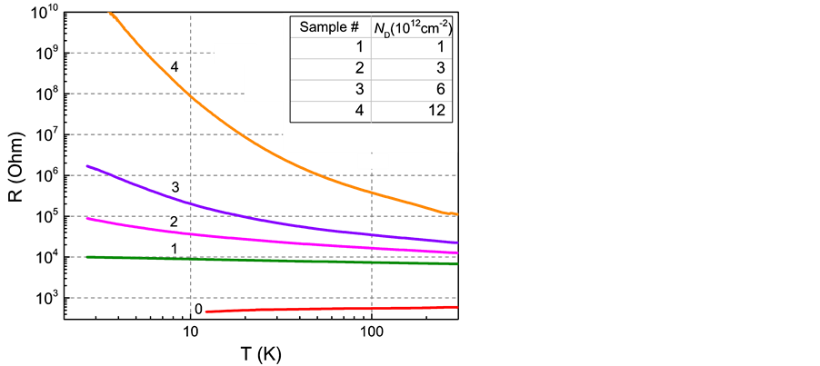
Figure 1. Resistivity of disordered monolayer graphene samples as a function of temperature. Inset shows the density of structural defects in samples [9] .

Figure 2. Magnetoconductance of sample 1 as function of magnetic field; solid lines―experiment, dashed lines―Equation (1) with fitted parameters.

Figure 3. Conductivity of sample 1 as function of temperature. Circles present experimental data, squares present Equation (2) with parameters determined from fitting the magnetoconductance (A was chosen to be ). The values of
  (solid line),
  (short-dashed line) and
  (long-dashed line, right axis).
Quantum corrections to the conductivity of graphene have been intensely studied theoretically [11] -[19] . It is predicted that at relatively high temperatures WAL corrections will dominate, while with decreasing T the WL corrections will dominate. There were several experimental papers reporting logarithmic dependence of conductivity on temperature and magnetic field at low temperatures [1] -[5] [7] . However, in our sample 1, the logarithmic dependence is observed in wide temperature interval, starting from 300 K, which gives an opportunity to check in a very detailed way the theoretical predictions. For the MC the theory [15] predicts
 (1)
(1)

where  is the digamma function,
  is the coherence time,
  is the intervalley scattering rate,
  is the combined scattering rate of intravalley and intervalley scattering and of trigonal warping.
The result of fitting Equation (1) to experimental data for magnetoconductance of sample 1 at different temperatures is illustrated on Figure 2. In the process of fitting we are able to extract all three parameters entering the equation, which are shown in inset in Figure 3. It turns out, that the parameters are temperature-dependent which is not predicted by theory. Using these parameters we can calculate conductance at zero magnetic field according to Equation (10) of [15] , which can be rewritten in the form
 (2)
(2)
where A is a constant, dependent upon the unit of magnetic field (chosen as 1T). We compare Equation (2) with the experimentally measured conductivity . The comparison is presented on Figure 3. The good agreement proves the correctness of the chosen parameters. The inset to Figure 3 shows that, apart from the lowest temperatures,
 . Mechanisms that can give such dependence are: electron-electron scattering in dirty limit [10] , electron-phonon scattering [20] [21] and electron-flexural phonon interaction [22] . The saturation of
  at low temperatures is well known in classical 2d systems and may be connected with existence of dephasing centers (for example, magnetic impurities) [23] [24] .Obtained value of
  allow us to determine the values of dephasing length
 . When the temperature decreases from 300 K to 3 K, the dephasing length
  increases from 7 nm to 70 nm and then saturates. The maximal value of
  allows us to estimate the density of dephasing centers as
  cm-2.
cm-2.
3. Strong Localization
Let’s discuss now samples 2 - 4 with pronounced insulating behavior. Plotting the data on the Arrhenius scale lnR vs. 1/T shows that energy of activation continuously decreases with decreasing T which is characteristic for the variable-range-hopping (VRH) conductivity [25] . There are two kinds of VRH depending on the structure of the density-of-states (DOS)  in the vicinity of the Fermi level (FL)
  when
when , R(T) is described by the Mott
  law in the case of two-dimensional (2d) conductivity
 (3)
(3)
Here  is the numerical coefficient [25] , a is the radius of localization.
The Coulomb interaction between localized carriers leads to appearance of the soft Coulomb gap in the vicinity of FL which in the case of 2d has a linear form
 (4)
(4)
where  is the dielectric constant of the material. This leads to the Efros-Shklovskii (ES) VRH or
  law
law
 (5)
(5)
where the numerical coefficient  [25] .
Coulomb interaction can alter the DOS only near the FL. Far from FL, the DOS is restored to its initial value, which is approximately equal to , see inset in Figure 4. Denoting the half-width of the Coulomb gap as
  one can conclude, therefore, that at
  ES law has to be observed, while in the opposite case
 , the Mott law should dominate.
There are a number of reports about observation of either Mott or ES laws in different disordered graphene- based materials [26] -[29] . We show that in samples 3 and 4, both VRH laws are observable at different temperatures (For sample 2, the VRH regime will be observed at lower temperatures). In Figure 4 and Figure 5, log R is plotted versus  and
and . At high temperatures, dependences R(T) are straightened on the scale
 , while at low temperatures they are straightened on the scale
 . The latter shows the approach to the ES law which should be observed at the lowest temperatures. These plots allow us to determine both parameters
  and
and  (Table 1) and calculate the temperature
  of deviation from
  law to
  law in the case of 2d conductivity similarly to the calculation of
  for 3d conductivity [30] . In VRH, only localized states in an optimal band of width
  near the Fermi level are involved in the hopping process. The band becomes continuously narrower with decreasing
 . Hopping resistance is determined by the critical parameter
 (6)
(6)
Here energy and temperature are measured in the same units, r is the mean distance of hopping. In the Mott regime,  and, therefore, the total number of states in the optimal band is
  and the mean distance between states in two dimensions is
 . Substituting in Equation (6), one can find from the minimal value of
  determined from
 ,
,
 (7)
(7)
This gives the relationship between  and the width of the optimal band:
 . At the crossover temperature Tc we get
 , so
, so
 (8)
(8)
Being inside the Coulomb gap, the crossover temperature can be determined from , which gives
 . Substituting into Equation (8) and using expressions for
  and
and , from Equation

Figure 4. Log R for samples 2 - 4 plotted versus .
.

Figure 5. Log R for samples 2 - 4 plotted versus .
.

Table 1. Hopping conductivity parameters for samples 3, 4.
(3) and Equation (5), we get
 (9)
(9)
The functional proportionality of  to the ratio
  has been obtained earlier [31] [32] , but with significantly different numerical coefficient. The latter is, however, crucial for comparison with experiment. The values of
  calculated from Equation (9) for samples 3 and 4 are given in Table 1 and shown as arrows in Figure 4. The good agreement shows the correctness of the obtained numerical coefficient. We can also estimate the width of the Coulomb gap. In calculation, the value
  for the monolayer graphene on the SiO2 surface was used as
 , where
  (for SiO2) and
  (for air). One can see that indeed, the ES law is observed when
 .
.
Comparison of samples 3 and 4 shows that increase of the density of defects  leads to stronger localization which manifests in a significant decrease of a and increase of the energy band needed for hopping. This looks like increase of the amplitude of the random potential relief in classical semiconductors induced by randomly distributed positively charged donors and negatively charged acceptors in the case of compensation. Hence, we assume that structural defects in graphene are of amphoteric impurity action [33] , i.e. they can be either acceptors or donors and compensate each other. Thus, increase of
  leads to the random potential relief amplitude increase.
One can also assume that this phenomenon may be connected with the fact that some point defects (say, vacancies) may produce complex associative centers with other defects. These associations can show an amphoteric impurity action, whereas the individual components are not amphoteric [34] .
In conclusion, a gradual transformation of conductivity measured in a wide interval of temperatures (300 - 1.8 K) and magnetic fields (up to 4 T) was observed in a series of monolayer graphene samples subjected by different dose of ion irradiation. Increase of the density of structural defects  induced by irradiation has led to change the mechanism of electron transport from metallic conductivity to the regime of WL and finally to the VRH of strongly localized carriers. It is shown that WL regime in slightly disordered sample starts from high (room) temperatures.
Comparison of experimental magnetoconductance curves with theory allows us to find the parameters which determine the logarithmic temperature dependence of conductivity in WL regime. In VRH, a crossover from the Mott law to the Efros-Shklovskii law is observed in the same samples with decreasing temperature. The calculated crossover temperatures are in good agreement with experimental values. It is suggested that strengthening of localization with increase of  can be explained by amphoteric impurity action of graphene structural defects induced by ion irradiation.
Cite this paper
ErezZion,AvnerHaran,AlexanderButenko,LeonidWolfson,YuriKaganovskii,TalHavdala,AmosSharoni,DoronNaveh,VladmirRichter,MosheKaveh,EugeneKogan,IssaiShlimak, (2015) Localization of Charge Carriers in Monolayer Graphene Gradually Disordered by Ion Irradiation. Graphene,04,45-53. doi: 10.4236/graphene.2015.43005
References
- 1. Morozov, S.V., Novoselov, K.S., Katsnelson, M.I., Schedin, F., Ponomarenko, L.A., Jiang, D. and Geim, A.K. (2006) Strong Suppression of Weak Localization in Graphene. Physical Review Letters, 97, Article ID: 016801. http://dx.doi.org/10.1103/physrevlett.97.016801
- 2. Wu, X.S., Li, X.B., Song, Z.M., Berger, C. and de Heer, W.A. (2007) Weak Antilocalization in Epitaxial Graphene: Evidence for Chiral Electrons. Physical Review Letters, 98, Article ID: 136801.
http://dx.doi.org/10.1103/physrevlett.98.136801 - 3. Tikhonenko, F.V., Kozikov, A.A., Savchenko, A.K. and Gorbachev, R.V. (2009) Transition between Electron Localization and Antilocalization in Graphene. Physical Review Letters, 103, Article ID: 226801. http://dx.doi.org/10.1103/PhysRevLett.103.226801
- 4. Chen, Y.-F., Bae, M.-H., Chialvo, C., Dirks, T., Bezryadin, A. and Mason, N. (2010) Magnetoresistance in Single-Layer Graphene: Weak Localization and Universal Conductance Fluctuation Studies. Journal of Physics: Condensed Matter, 22, Article ID: 205301.
http://dx.doi.org/10.1088/0953-8984/22/20/205301 - 5. Lundeberg, M.B. and Folk, J.A. (2010) Rippled Graphene in an In-Plane Magnetic Field: Effects of a Random Vector Potential. Physical Review Letters, 105, Article ID: 146804.
http://dx.doi.org/10.1103/physrevlett.105.146804 - 6. Buchowicz, G., Stone, P.R., Robinson, J.T., Cress, C.D., Beeman, J.W. and Dubon, O.D. (2011) Correlation between Structure and Electrical Transport in Ion-Irradiated Graphene Grown on Cu Foils. Applied Physics Letters, 98, Article ID: 032102.
http://dx.doi.org/10.1063/1.3536529 - 7. Jobst, J., Waldmann, D., Gornyi, I.V., Mirlin, A.D. and Weber, H.B. (2012) Electron-Electron Interaction in the Magnetoresistance of Graphene. Physical Review Letters, 108, Article ID: 106601. http://dx.doi.org/10.1103/PhysRevLett.108.106601
- 8. Moktadir, Z., Hang, S.J. and Mizuta, H. (2014) Defect-Induced Fermi Level Pinning and Suppression of Ambipolar Behaviour in Graphene. http://arxiv.org/abs/1410.4400
- 9. Shlimak, I., Haran, A., Zion, E., Havdala, T., Kaganovskii, Yu., Butenko, A.V., Wolfson, L., Richter, V., Naveh, D., Sharoni, A., Kogan, E. and Kaveh, M. (2015) Raman Scattering and Electrical Resistance of Highly Disordered Graphene. Physical Review B, 91, Article ID: 045414.
http://dx.doi.org/10.1103/physrevb.91.045414 - 10. Altshuler, B.L., Aronov, A.G. and Khmelnitsky, D.E. (1982) Effects of Electron-Electron Collisions with Small Energy Transfers on Quantum Localization. Journal of Physics C: Solid State Physics, 15, Article ID: 7367. http://dx.doi.org/10.1088/0022-3719/15/36/018
- 11. Morpurgo, A.F. and Guinea, F. (2006) Intervalley Scattering, Long-Range Disorder, and Effective Time-Reversal Symmetry Breaking in Graphene. Physical Review Letters, 97, Article ID: 196804. http://dx.doi.org/10.1103/PhysRevLett.97.196804
- 12. Aleiner, I.L. and Efetov, K.B. (2006) Effect of Disorder on Transport in Graphene. Physical Review Letters, 97, Article ID: 236801. http://dx.doi.org/10.1103/PhysRevLett.97.236801
- 13. Altland, A. (2006) Low-Energy Theory of Disordered Graphene. Physical Review Letters, 97, Article ID: 236802. http://dx.doi.org/10.1103/PhysRevLett.97.236802
- 14. Ostrovsky, P.M., Gornyi, I.V. and Mirlin, A.D. (2006) Electron Transport in Disordered Graphene. Physical Review B, 74, Article ID: 235443.
http://dx.doi.org/10.1103/PhysRevB.74.235443 - 15. McCann, E., Kechedzhi, K., Fal’ko, V.I., Suzuura, H., Ando, T. and Altshuler, B.L. (2006) Weak-Localization Magnetoresistance and Valley Symmetry in Graphene. Physical Review Letters, 97, Article ID: 146805. http://dx.doi.org/10.1103/PhysRevLett.97.146805
- 16. Kechedzhi, K., McCann, E., Fal’ko, V.I., Suzuura, H., Ando, T. and Altshuler, B.L. (2007) Weak Localization in Monolayer and Bilayer Graphene. The European Physical Journal Special Topics, 148, 39-54. http://dx.doi.org/10.1140/epjst/e2007-00224-6
- 17. Tikhonenko, F.V., Kozikov, A.A., Savchenko, A.K. and Gorbachev, R.V. (2009) Transition between Electron Localization and Antilocalization in Graphene. Physical Review Letters, 103, Article ID: 226801. http://dx.doi.org/10.1103/PhysRevLett.103.226801
- 18. Pal, A.N., Kochat, V. and Ghosh, A. (2012) Direct Observation of Valley Hybridization and Universal Symmetry of Graphene with Mesoscopic Conductance Fluctuations. Physical Review Letters, 109, Article ID: 196601.
http://dx.doi.org/10.1103/PhysRevLett.109.196601 - 19. Baker, A.M.R., Alexander-Webber, J.A., Altebaeumer, T., Janssen, T.J.B.M., Tzalenchuk, A., Lara-Avila, S., Kubatkin, S., Yakimova, R., Lin, C.-T., Li, L.-J. and Nicholas, R.J. (2012) Weak Localization Scattering Lengths in Epitaxial, and CVD Graphene. Physical Review B, 86, Article ID: 235441.
http://dx.doi.org/10.1103/PhysRevB.86.235441 - 20. Stauber, T., Peres, N.M.R. and Guinea, F. (2007) Electronic Transport in Graphene: A Semiclassical Approach Including Midgap States. Physical Review B, 76, Article ID: 205423.
http://dx.doi.org/10.1103/physrevb.76.205423 - 21. Hwang, E.H. and Das Sarma, S. (2008) Acoustic Phonon Scattering Limited Carrier Mobility in Two-Dimensional Extrinsic Graphene. Physical Review B, 77, Article ID: 115449.
http://dx.doi.org/10.1103/PhysRevB.77.115449 - 22. Tikhonov, K.S., Zhao, W.L.Z. and Finkelstein, A.M. (2014) Dephasing Time in Graphene Due to Interaction with Flexural Phonons. Physical Review Letters, 113, Article ID: 076601.
http://dx.doi.org/10.1103/PhysRevLett.113.076601 - 23. Bishop, D.J., Tsui, D.C. and Dines, R.C. (1980) Nonmetallic Conduction in Electron Inversion Layers at Low Temperatures. Physical Review Letters, 44, Article ID: 1153.
- 24. Gantmakher, V.F. (2005) Electrons and Disorder in Solids. Oxford University Press, Oxford.
http://dx.doi.org/10.1093/acprof:oso/9780198567561.001.0001 - 25. Shklovskii, B.I. and Efros, A.L. (1984) Electronic Properties of Doped Semiconductors. Springer-Verlag, Berlin. http://dx.doi.org/10.1007/978-3-662-02403-4
- 26. Moser, J., Tao, H., Roche, S., Alzina, F., Sotomayor Torres, C.M. and Bachtold, A. (2010) Magnetotransport in Disordered Graphene Exposed to Ozone: From Weak to Strong Localization. Physical Review B, 81, Article ID: 205445.
http://dx.doi.org/10.1103/PhysRevB.81.205445 - 27. Joung, D. and Khondaker, S. (2012) Efros-Shklovskii Variable-Range Hopping in Reduced Graphene Oxide Sheets of Varying Carbon sp2 Fraction. Physical Review B, 86, Article ID: 235423.
http://dx.doi.org/10.1103/PhysRevB.86.235423 - 28. Hong, X., Cheng, S.-H., Herding, C. and Zhu, J. (2011) Colossal Negative Magnetoresistance in Dilute Fluorinated Graphene. Physical Review B, 83, Article ID: 085410.
http://dx.doi.org/10.1103/PhysRevB.83.085410 - 29. Zhang, H.J., Lu, J.M., Wu, S., Wang, Z., Zhang, T., Sun, M.Y., Zheng, Y., Chen, Q.H., Wang, N., Lin, J.J. and Sheng, P. (2013) Large-Scale Mesoscopic Transport in Nanostructured Graphene. Physical Review Letters, 110, Article ID: 066805.
http://dx.doi.org/10.1103/physrevlett.110.066805 - 30. Shlimak, I., Kaveh, M., Yosefin, M., Lea, M. and Fozooni, P. (1992) Crossover Phenomenon for Hopping Conduction in Strong Magnetic Fields. Physical Review Letters, 68, Article ID: 3076.
- 31. Singh, M., Tarutani, Y., Kabasava, U. and Takagi, K. (1994) Temperature and Electric-Field Dependence of Hopping Transport in Low-Dimensional Devices. Physical Review B, 50, 7007-7015.
http://dx.doi.org/10.1103/PhysRevB.50.7007 - 32. Lien, N.V. (1995) Crossovers in Two-Dimensional Variable Range Hopping. Physics Letters A, 207, 379-384.
- 33. Dunlap, W.C. (1955) Amphoteric Impurity Action in Germanium. Physical Review, 100, 1629-1633. http://dx.doi.org/10.1103/PhysRev.100.1629
- 34. Fistul, V. (2004) Impurities in Semiconductors: Solubility, Migration and Interactions. CRS Press, Boca Raton. http://dx.doi.org/10.1201/9780203299258
NOTES

*Corresponding author.