Crystal Structure Theory and Applications
Vol. 2 No. 2 (2013) , Article ID: 33049 , 7 pages DOI:10.4236/csta.2013.22006
ZnO Heteroepitaxy on Sapphire Using a Novel Buffer Layer of Titanium Oxide: Crystallographic Behavior
1Department of Biomolecular Functional Engineering, Ibaraki University, Hitachi, Japan
2Department of Electric and Electronic Engineering, Ibaraki University, Hitachi, Japan
Email: *ysatoshi@mx.ibaraki.ac.jp
Copyright © 2013 Satoshi Yamauchi, Yoh Imai. This is an open access article distributed under the Creative Commons Attribution License, which permits unrestricted use, distribution, and reproduction in any medium, provided the original work is properly cited.
Received October 31, 2012; revised January 2, 2013; accepted January 11, 2013
Keywords: ZnO; Ti2O3; Plasma-Assisted Epitaxy; Hexagonal Pyramid Grain
ABSTRACT
A novel buffer layer consists of titanium oxide grown on a-sapphire by low-pressure chemical vapor deposition using titanum-tetra-iso-propoxide and oxygen gas was used for ZnO epitaxial growth at temperature as low as 340˚C by plasma-assisted epitaxy using radio-frequency oxygen-gas plasma. XRD and RHEED indicated (0001)Ti2O3 layer in corundum crystal system was epitaxially grown on the substrate in an in-plane relationship of [1-100]Ti2O3// [0001]Al2O3 by uniaxial phase-lock system. Growth behavior of ZnO layer was significantly dependent on the Ti2O3 buffer-layer thickness, for example, dense columnar ZnO-grains were grown on the buffer layer thinner than 10 nm but the hexagonal pyramid-like grains were formed on the thin buffer layers below 2 nm. RHEED observations showed ZnO layer including the pyramid-like grains was epitaxially grown with single-domain on the thin buffer layer of 0.8 nm in the in-plane relationship of [1-100]ZnO//[1-100]Ti2O3//[0001]Al2O3, whereas the multi-domain was included in ZnO layer on the buffer layer above 10 nm.
1. Introduction
ZnO has been candidate of interesting material for highly efficient blue or ultraviolet light-emitting devices because of the wide direct band gap of 3.37 eV at room temperature and the large exciton binding energy of 60 meV. However, it has been recognized that undopedZnO shows highly n-type conductivity by native-defects such as interstitial-Zn and strong green emission due to oxygen deficiency, which are introduced by the high temperature growth and/or poor reactivity of supplied oxygen for the growth. Several advanced processes such as Moleculer-Beam Epitaxy (MBE) using oxygen-plasma cell [1], Metal-Organic MBE (MOMBE) using H2O vapor [2], Pulsed Laser Deposition (PLD) [3] etc. have been developed to reduce the native defects. Plasmaassisted epitaxy (PAE) using oxygen plasma excited by radio-frequency (rf) power is also useful to achieve ZnOepitaxial growth at low temperatures supplying reactive oxygen as demonstrated for undoped-ZnO growth at 400˚C on c-sapphire [4,5] and Si [6]. In addition, acceptor-doping with sufficient dopant preventing the selfcompensation should be required to fabricate p-type ZnO and the pn-junction. Nitrogen has been used for acceptor-doping into ZnO layer [2,7] including the co-doping [8], however, the heavily doped nitrogen-acceptor showed the large activation energy such as 224 meV [9]. In contrast, relatively shallow nitrogen acceptor with the activation energy of 132 meV was doped into ZnO layer by PAE using O2 + N2 gas plasma with precise control of O/Zn supply ratio during the growth [10]. Such features have been observed in the growth of other II-VI compound semiconductor such as ZnSe [11] and are originnated from self-compensation in the heavy acceptordoping by native donor-defects. For ZnO growth, the growth mode should be taken into account to control the doping since the layer has been grown on sapphire substrate with large lattice mismatching. Indeed, it was reported that the electron concentration is high in ZnO layers including three-dimensional grains and/or multi-domains [12], where the donor defects were probably come from interstitial-Zn formed on the three-dimensional surface with higher sticking coefficient of Zn on the steps and kinks. In general, suitable buffer layer is required for two-dimensional epitaxial growth in lattice mismatching system such as ZnO/sapphire to satisfy the relationship of σsv > σsc + σcv by reducing the interface energy, where σsv, σsc and σcv are surface energy on the substrate, interface energy and surface energy of film respectively. For the purpose, Y. Chen et al. reported interest results to relax the lattice-mismatching by using an initial buffer layer of thin MgO layer with rocksalt crystal structure on c-sapphire, where the mismatch could be reduced to 9% comparing the large value of 18% on c-sapphire [13]. In the hetero-epitaxial system, initial ZnO layer grown at 500˚C on the buffer layer was annealed at 750˚C to reduce the surface roughness, and then single domain ZnO layer was epitaxially grown with smooth surface at 620˚C. However, it was also reported that the low temperature photoluminescence spectrum was improved but dominated by neutral donor-bound exciton emission at 3.369 eV, which indicates native donor was still included in the ZnO layer. In contrast, while Ti2O3 with corundum crystal structure is also an interesting material as the initial buffer layer, which is expected to reduce the lattice mismatch in the system of (0001)ZnO/(0001)Ti2O3 as low as 5% with large surface energy on the (0001)Ti2O3, the heteroepitaxial system has not been studied because Ti2O3 single has not been established.
In this paper, we demonstrate epitaxial growth of Ti2O3 layer on a-sapphire by low-pressure chemical vapor deposition and then enhanced two-dimensional epitaxial growth of ZnO layer at the temperature as low as 340˚C by PAE on the Ti2O3 buffer layer.
2. Experimental
Titanium oxide layer was grown in bell-jar type chamber at low temperature of 320˚C in 3 mtorr on a-sapphire by LPCVD using titanium tetra-iso-propoxide (TTIP: Ti- (OC3H7)4) and oxygen gas. The liquid TTIP (97% purity) was vaporized in a quartz-cell at 70˚C after purification in vacuum at 50˚C for 3 hr, then the TTIP-gas was introduced into the growth chamber through a hot alumina nozzle at 85˚C monitoring and controlling the pressure in the chamber using Schultz gage and a variable valve, where high-purity oxygen gas (6N-purity) was simultaneously supplied with the TTIP-gas but through the individual gas lines for precise control O2/TTIP supply ratio. It is mentioned here that detection sensitivity in such ion-gage should be corrected for each gas species to determine the supply rate but the directly monitored pressure was used without the correction in this study because it is not easy to evaluate the sensitivity of the metal-organic gas catalyzed by the oxidant.
ZnO layer was grown at 340˚C in 3 mtorr by plasmaassisted epitaxy (PAE) using oxygen gas plasma which was excited by 10 W rf-power at 13.56 MHz using a capacitively coupled rf-electrode. Details of the PAE apparatus were described elsewhere [9]. High-purity elemental Zn (6N-up purity) and oxygen gas (6N purity) were used for ZnO growth. Elemental Zn (6N-up purity) was evaporated from a Knudsen cell with a nozzle to prevent oxidation of the surface and supplied to the growth surface through the oxygen gas plasma, where high-purity oxygen gas with 6N-purity was used. Effective Zn/O supply ratio was determined by the dependence of ZnO growth rate on Zn-supply rate [9].
300 m-thick single crystalline aand c-sapphire with mirror surface used as substrates were cleaned in organic-solvents and hot H2SO4 + H2O2 at 60˚C for 5 min, then, loaded into the chamber after rinse in ultra purewater with the resistivity above 18.2 M cm and blow by nitrogen-gas. In the case of substrate etching, a hot 3H2SO4 + H3PO4 solution at 130˚C was used as the etchant and the substrate treated by H2SO4 + H2O2 was etched for 15 min.
Thickness of the titanium-oxide layer and the ZnO layer were checked by a contact-type surface profiler, where the thickness of the thin titanium-oxide layer below 10 nm was estimated by the growth rate evaluated for the layer above 20 nm-thickness and the period rate. Crystal-system and crystal-orientation was examined by a-2XRD measurement using Cuk1,2. Surface morphology of the ZnO films was observed by Nomarski differential interference microscope. Reflection high-energy electron diffraction (RHEED) system was also used on the surfaces of the layers and the substrate to disclose the surface structures and the in-plane epitaxial relationship.
3. Results and Discussions
3.1. Ti2O3 Epitaxial Growth on A-Sapphire
It is recognized that titanium-oxide growth using TTIP and O2 is owing to thermal catalysis of TTIP enhanced by the oxidation, therefore, the growth behavior includeing the crystallinity is significantly dependent on not only the growth temperature but also the supply ratio of O2/TTIP [14]. As a typical result, FTIR results indicated that some types of impurities such as hydrocarbons and hydroxyls derived from the TTIP dissociation sequences were slightly remained in the layer by the low supply ratio below 1 but not detected in the layer grown by O2-rich conditions above 1.5, therefore, the layer was grown in the large supply ratio of 8 to remove such impurities completely. On the other, it has also been recognized that titanium oxide compound can be crystallized in diverse compositions and crystal systems due to the hybrid-orbital of titanium including the d-orbital, where the valence of Ti is changed from 0.33 to 5.0. Tokita et al. reported (112) anatase-TiO2 with tetragonal crystal system can be epitaxially grown on c-sapphire at relatively low temperature about 500˚C by atmospheric chemical vapor deposition using TTIP and O2 [15]. In contrast, we found out (0001) Ti2O3 with corundum in hexagonal system was epitaxially grown on a-sapphire by LPCVD as shown below. Figure 1 shows XRD profile of 400 nm-thick titanium-oxide layer grown on a-sapphire by LPCVD, where the diffraction corresponding to (0006)Ti2O3 was only appeared at 39.5˚ [16] from the layer with some peaks from the substrate, which indicates preferentially (0001) oriented Ti2O3 layer was grown on the substrate. Figures 2(a) and (b) show RHEED patterns of the layer with the thickness of 10 nm, where the electron beam was incident along [0001]Al2O3 and [1-100]Al2O3, respectively. It is noted that the patterns corresponding to (a) [1-100] and (b) [-1-120]Ti2O3 showed sixfold-symmetry because each pattern was repeated every 60˚ and alternated every 30˚ when the film was rotated with respect to the electron beam incident. The RHEED patterns showed the layer was three-dimensional growth but clearly indicated (0001)Ti2O3 layer was epitaxially grown on a-sapphire with an inplane relationship of [1-100]Ti2O3//[0001]Al2O3. Representation of oxygen in the two surfaces can be shown as Figure 3, where the oxygen on Al2O3 and Ti2O3 surface is shown by open and closed circles, respectively. The symmetry of the oxygen arrangement between the two surfaces was different in each other, however, the distance of oxygen on Ti2O3 is periodically matched along [1-100]Al2O3, in which the threefold oxygen on Ti2O3 surface along [1100]Ti2O3 is just matched to the fivefold oxygen in Al2O3 along [1-100]Al2O3 with the mismatch less
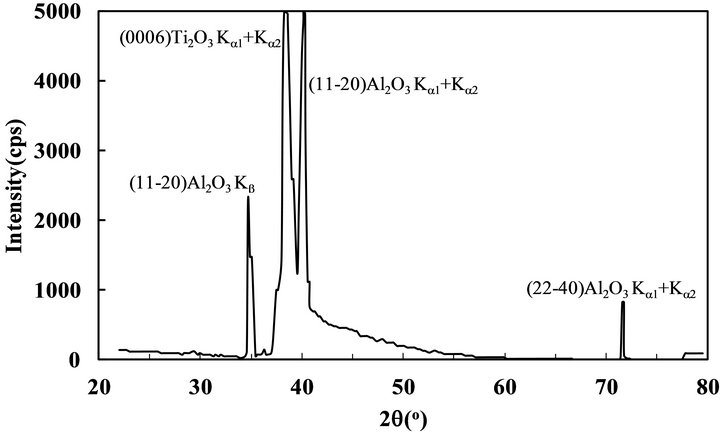
Figure 1. θ - 2θ XRD pattern of 400 nm-thick Ti2O3 layer grown on a-sapphire by LPCVD.
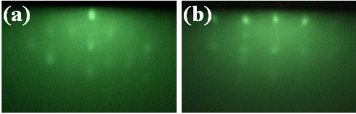
Figure 2. RHEED patterns on Ti2O3 layer grown on a-sapphire, where the electron beam was incident along (a) [0001] and (b) [1-100]Al2O3.
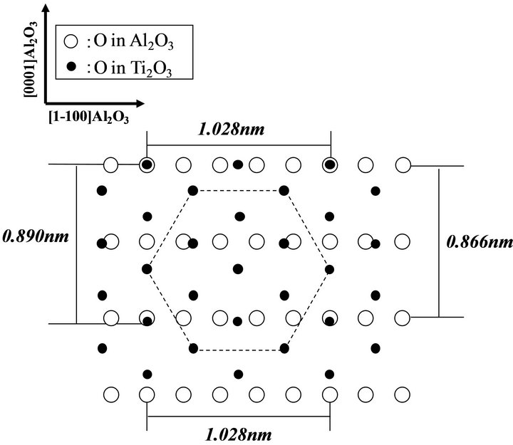
Figure 3. Representation of oxygen on a-sapphire (opencircles) and (0001)Ti2O3 (closed-circles) in the in-plane relationship of [1-100]Ti2O3//[0001]Al2O3.
than 0.06% in addition to the relatively low mismatching of 2.8% along [0001]Al2O3. Previously, it was demonstrated that (0001)ZnO with sixfold-symmetry is locked by uniaxially matched oxygen along [0001]Al2O3 with twofold symmetric oxygen on a-sapphire surface [17]. Also in the Ti2O3/a-sapphire system, it can be considered that (0001)Ti2O3 was locked by the asymmetry on a-sapphire surface along [1-100]Al2O3. The spotty RHEED patterns as shown in Figure 2 were significantly dependent on the layer thickness as shown in Figure 4, which showed RHEED patterns of (a) 2 nmand (b) 0.8 nm-thick Ti2O3 layers, where the electron beam was incident along [1-100]Al2O3 as same as Figure 2(b). The spotty pattern from the relatively thick layer above 10 nm (Figure 2(b)) was changed to streak with decreasing the thickness below 2 nm and showed the fine Kikuchi-line on the 0.8 nm-thick layer.
The sixfold symmetry observed for the 10 nm-thick layer was same as the very thin layers, however, the streak-line distance for the 0.8 nm-thick layer was slightly large (about 2%) comparing to that for the thick layer, which suggested the layer was stressed by the lattice mismatch along [1-100]Al2O3. These results indicated the layer was two-dimensionally grown with slightly shrunk hexagonal unit at initial stage but three-dimensionally above the critical thickness probably within the lattice constant along c-axis (1.364 nm). The growth features can be considered that the layer was grown by Stranski-Krastanov mode [18], in which the energy relationship between the substrate and the layer is satisfied to be σsv > σsc + σcv for the thickness below the critical thickness but changed to be σsv < σsc + σcv for the layer thicker than the critical thickness, or secondary nucleation caused by dislocation in the layer grown on the lattice mismatched substrate. Of course, the growth behaveior of Ti2O3 layer including the critical thickness was
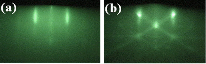
Figure 4. RHEED patterns of Ti2O3 layer with the thickness of (a) 2 nm and (b) 0.8 nm on a-sapphire, where the electron beam was incident along [1-100]Al2O3.
significantly influenced by the growth conditions such as the introduced gas rate, growth temperature and so on, and the thin layer with smooth surface as shown in Figure 4(b) could be grown in oxygen rich condition (O2/TTIP supply ratio above 8) with the low growth rate about 0.3 nm/min at 320˚C.
3.2. ZnO Growth on Ti2O3 Buffer Layer
3.2.1. Surface Morphology
Figure 5 shows Nomarski-photographs of PAE-ZnO layers with the thickness about 600 nm grown at 340˚C. Preferentially (0001) oriented ZnO layer consists of densely three-dimensional columnar grains was grown on csapphire (Figure 5(a)), however, the 30˚-rotational domains with in-plane relationships of [11-20]ZnO//[11- 20]Al2O3 and [10-10]ZnO//[11-20]Al2O3 due to large lattice mismatch between (0001)ZnO and c-sapphire were included in the layer as reported elsewhere [19]. In contrast, polycrystalline ZnO layer with rough surface including (10-11) and (0001) oriented grains was grown on a-sapphire at the temperature as low as 340˚C by PAE, while single-crystalline (0001)ZnO layer was grown on a-sapphire at 500˚C by radical source MBE using two step process demonstrated by the initial step for nucleation at 400˚C and the in-situ annealing for the coalescence at 500˚C [17]. It is considered that the growth behavior on a-sapphire by PAE was come from three-dimensional nucleation with the low density at the initial stage, which was resulted in textured three-dimensional grain growth and secondary nucleation in deep grain boundaries on the ZnO surface during the growth. In contrast, the feature on the Ti2O3 layer was quite differed as shown in Figures 5(c)-(e), where ZnO layer with the average thickness about 600 nm was grown at 340˚C. ZnO layer consists of highly dense columnar grains coming from high density nucleation on the Ti2O3 layer comparing to that on sapphires was grown on the buffer layer above 10 nm (Figure 5(c)), which speculated that the surface reactivity of the layer was higher than sapphire. Further, pyramid-shape grains with the hexagonal facets could be clearly observed in the ZnO layers on the thinner Ti2O3 layer than 2 nm and the density was decreased with decreasing the buffer layer thickness (Figures 5(d) and (e)). It is interesting that
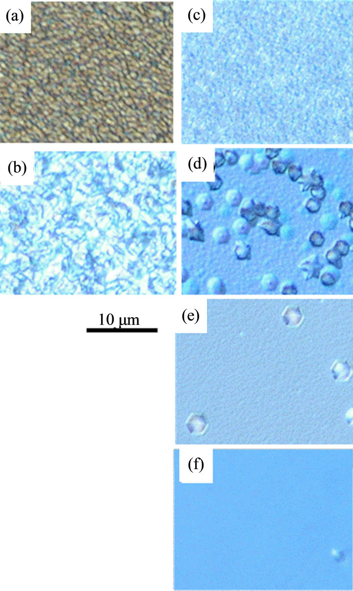
Figure 5. Surface morphologies observed by Nomarski microscope of ZnO layers on (a) c-sapphire, (b) a-sapphire, (c) 10 nm-thick buffer layer, (d) 2 nm-thick buffer layer, (e) 0.8 nm-thick buffer layer on a-sapphire and (f) 0.8 nm-thick buffer layer on a-sapphire etched by 3H2SO4 + H3PO4 solution.
the small columnar-like grain was observed at center of the pyramid in the layer on 2 nm-thick buffer layer (Figure 5(d)), which was expected the three-dimensional nuclei was firstly created at the initial stage and then the pyramid grain grew around the columnar-like grain, that is, the columnar-like grain was grown with significantly higher rate comparing to the smooth surface. The pyramid was also formed in ZnO layer on the 0.8 nm-thick Ti2O3 layer but the columnar-like grain in the center could not be observed, which indicates growth rate of the columnar-like grain was lower than that on the 2 nmthick Ti2O3 layer. Figure 6 shows growth rates of ZnO layer on c-sapphire and the 0.8 nm-thick buffer layer as a function of Zn evaporated rate from the cell during the growth in constant O2-supply rate and induced rf-power, where the growth rate was evaluated by the thickness of ZnO layer grown for 1 hour and the thickness on the buffer layer was checked on the smooth surface without the pyramids. In both cases, the growth rate was limited by the smaller supply rate of Zn or O, which indicated the sticking coefficients of Zn on Zn and O on O were negligible in this condition, but obviously larger on c-sapphire than on the buffer layer. On the other, both of the saturated growth rate in the height and the Zn-flux for
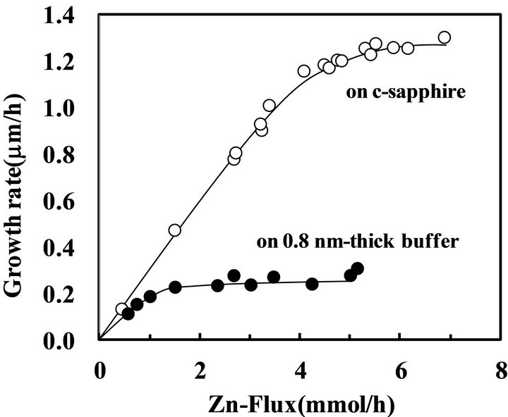
Figure 6. Growth rate of ZnO layer on c-sapphire and 0.8 nm-thick buffer layer.
the effective supply rate of Zn/O = 1 were increased for the pyramids. In addition, the values were increased with the buffer thickness, for example, the pyramids were grown with the rate about 0.7 m/h by the Zn-flux above 2.5 mm/h on the 0.8 nm-thick layer but about 1 m/h by the flux above 3.5 mmol/h on the 2 nm-thick layer. It is noted here that the ZnO layer consists of columnar grains on the thick buffer layer above 10 nm was grown with the high rate comparable to that on c-sapphire. Previously, it was reported that growth rate of ZnO layer on Zn-polar surface is higher than that on O-polar surface [20] because of the higher sticking coefficient of O-adatom on the Zn-face than that of Zn-adatom on the O-face. If the high growth rate of the partially formed pyramid grain comparing to the other smooth area was originated from the growth faces, it is expected the grain could not be formed with the fine hexagonal facets and the in-plane size should be determined at initial growth stage of ZnO, however, the grains showed the fine facets and the in-plane size were increased with the growth period. Therefore, it should be concluded that the high rate growth of the pyramid grains was not caused by difference of the polar on the growth surface but by the higher sticking coefficient of adatoms at the steps or the kinks than that on the terraces. The growth feature of the pyramid grain was also dependent on the surface condition of sapphire substrate, for example, the pyramid grain was almost disappeared by chemical etching of a-sapphire in a hot 3H2SO4 + H3PO4 solution at 130˚C for 15 min. as shown in Figure 5(f), where the growth conditions and the thickness for ZnO and Ti2O3 layers were same as the sample in Figure 5(e). The result clearly indicated that some types of defect including surface roughness on the buffer layer could be removed by the etching.
3.2.2. Epitaxial Relationship
Figure 7 show RHEED patterns corresponding to (a) [1-210] and (b) [-1010]ZnO on the ZnO layer shown in Figure 5(e) when the electron beam was incident along
Figure 7. RHEED patterns of ZnO layer on 0.8 nm-thick buffer layer when the electron beam was incident along (a) [0001] and (b) [1-100]Al2O3.
[0001] and [1-100]Al2O3, respectively. The each pattern was repeated every 60˚ and alternated every 30˚ as the film was rotated with respect to the electron beam incident. The patterns clearly indicated that the ZnO layer was epitaxially grown without rotational domains on the buffer layer, whereas the layer was including hexagonal pyramids. [1-210] of the hexagonal pyramids as shown in Figure 5(e) was also coincident to [0001]Al2O3. These results investigate the three-dimensional nuclei were partially formed with the same in-plane epitaxial relationship of the two-dimensional growth surface. As a result, the in-plane pyramid size could be increased with the growth period. The growth behavior is seemed that the ZnO layer was grown by two growth modes of Frank-van der Merwe [17] (two-dimensional growth) and VolmerWeber [18] (three-dimensional pyramid grain growth). It is considered that the three-dimensional nuclei might be originated from the surface defects of buffer layer, which was come from sapphire-substrate, and prevented by the surface treatment of the substrate such as the high-temperature annealing.
Figures 8(a) and (b) show schematic representations of oxygen on (0001)Ti2O3 and (0001)ZnO surfaces, where the oxygen-atoms on Ti2O3 and ZnO were shown by closedand open-circle with the unit cell by dot-line and solid-line hexagon based on the a-axis lattice constant of 0.324 nm and 0.514 nm for ZnO and Ti2O3, respectively. In the case of [1-210]ZnO//[1-100]Ti2O3 (Figure 8(a)), hexagon unit of the ZnO is larger than subunit hexagon of the Ti2O3 (about +9.2%), which is much smaller than that between (0001)ZnO/(0001)Al2O3 in the relationship of [1-210]ZnO//[1-100]Al2O3 (more than +18%). In contrast, the mismatch between the ZnO and the Ti2O3 with in-plane relationship of [1-100]ZnO// [1-100]Ti2O3 as shown in Figure 8(b) is reduced to −5.4% which is better than that in [1-210]ZnO//[1- 100]Ti2O3, therefore, the in-plane epitaxial relationship resulted in [1-100]ZnO//[1-100]Ti2O3. It is noted here that the mismatches between the ZnO and the 0.8 nm-thick Ti2O3 layer were expected to be smaller (about 2%) than the values because the hexagon unit at the 0.8 nm-thick Ti2O3 surface was slightly smaller than that of the bulk but the mismatch is estimated to be above 3%, however, the mismatch was still larger than that of (0001)ZnO/(0001)Al2O3 in the relationship of [1-100]ZnO
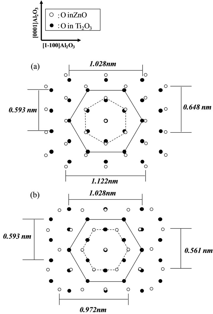
Figure 8. Representation of oxygen on (0001)Ti2O3 (closedcircles) and (0001)ZnO (open-circles) in the in-plane relationship of (a) [1-210]ZnO//[1-100]Ti2O3 and (b) [1-100]ZnO //[1-100]Ti2O3.
//[1-100]Al2O3 (about −2.3%). It has been commonly recognized that the phase-locking without rotational domain is difficult on c-sapphire with the isotropic hexagonal surface, but the results in this study indicated the phase could be successfully locked on the isotropic hexagonal surface of Ti2O3 layer. The useful results for ZnO growth on the buffer layer can be concluded that the phase-locking is performed not only by the latticematching but also by control of the surface chemistry on the mismatching substrate such as Ti2O3.
4. Conclusion
PAE-ZnO growth at low temperature of 340˚C was demonstrated on a-sapphire using a novel buffer layer consists of Ti2O3. (0001)Ti2O3 layer was epitaxially grown by LPCVD using TTIP and O2 on a-sapphire in the in-plane relationship of [1-100]Ti2O3//[0001]Al2O3 at 320˚C. Surface roughness of the Ti2O3 layer was increased with the thickness, however, extremely smooth surface could be obtained on thin buffer layer below 1 nm-thickness. The ZnO layer could be epitaxally grown with single domain in the in-plane relationship of [1- 100]ZnO//[1-100]Ti2O3 on the thin buffer layer. Hexagonal pyramid-shape ZnO grains by three-dimensional epitaxial growth were formed on the thin buffer layer in the in-plane epitaxial relationship with the significant high growth rate comparing to the two-dimensional growth. It was suggested from growth feature of the pyramid grains that epitaxial relationship in the three-dimensional growth was same as the two-dimensional growth and the high growth rate of the pyramid was caused by high sticking coefficient of adatoms on the three-dimensional surface. The number of the pyramid-grains could be obviously reduced by chemical wet etching of a-sapphire using hot 3H2SO4 + H3PO4 solution. The total-epitaxial relationship was revealed as [1-100]ZnO//[1-100]Ti2O3//[0001]Al2O3 by RHEED observations. These crystallographic results can be concluded that Ti2O3 layer is a promised candidate for the buffer layer to achieve high-quality ZnO growth at low temperatures.
REFERENCES
- M. A. L. Johnson, et al., “MBE Growth and Properties of ZnO on Sapphire and SiC Substrates,” Journal of Electronic Materials, Vol. 25, No. 5, 1996, pp. 855-862. doi:10.1007/BF02666649
- A. B. M. A. Ashrafi, et al., “Nitrogen-Doped p-Type ZnO Layers Prepared with H2O Vapor-Assisted Metalorganic Molecular-Beam Epitaxy,” Japanese Journal of Applied Physics, Vol. 41, 2002, pp. L1281-L1284. doi:10.1143/JJAP.41.L1281
- R. D. Vispute, et al., “High Quality Crystalline ZnO Buffer Layers on Sapphire(001) by Pulsed Laser Deposition for III-V Nitrides,” Applied Physics Letters, Vol. 70, No. 20, 1997, pp. 2735-2737. doi:10.1063/1.119006
- S. Yamauchi, et al., “Low Temperature Epitaxial Growth of ZnO Layer by Plasma-Assisted Epitaxy,” Thin Solid Films, Vol. 345, No. 1, 1999, pp. 12-17. doi:10.1016/S0040-6090(99)00096-6
- S. Yamauchi, et al., “Plasma-Assisted Epitaxial Growth of ZnO Layer on Sapphire,” Journal of Crystal Growth, Vol. 214-215, 2000, pp. 63-67. doi:10.1016/S0022-0248(00)00060-9
- S. Yamauchi, et al., “Surface Treatment of Si Using Hydrogen-Plasma to Improve Optoelectronic Property of ZnO on (111)Si,” Japanese Journal of Applied Physics, Vol. 44, 2005, pp. 7801-7804. doi:10.1143/JJAP.44.7801
- K. Minegishi, et al., “Growth of p-Type Zinc Oxide Films by Chemical Vapor Deposition,” Japanese Journal of Applied Physics, Vol. 36, 1997, pp. L1453-L1455. doi:10.1143/JJAP.36.L1453
- M. Joseph, et al., “p-Type Electrical Conduction in ZnO Thin Films by Ga and N Codoping,” Japanese Journal of Applied Physics, Vol. 38, 2001, pp. L1205-L1207. doi:10.1143/JJAP.38.L1205
- D. C. Look, et al., “Characterization of Homoepitaxial p-Type ZnO Grown by Molecular Beam Epitaxy,” Applied Physics Letters, Vol. 81, No. 10, 2002, pp. 1830- 1832. doi:10.1063/1.1504875
- S. Yamauchi, et al., “Photoluminescence Studies of Undoped and Nitrogen-Doped ZnO Layers Grown by Plasma-Assisted Epitaxy,” Journal of Crystal Growth, Vol. 260, No. 1-2, 2006, pp. 1-6. doi:10.1016/j.jcrysgro.2003.08.002
- I. S. Hauksson, et al., “Compensation Processes in Nitrogen Doped ZnSe,” Applied Physics Letters, Vol. 61, No. 18, 1992, pp. 2208-2210. doi:10.1063/1.108296
- A. Ohtomo, et al., “Lateral Grain Size and Electron Mobility in ZnO Epitaxial Films Grown on Sapphire Substrates,” Journal of Crystal Growth, Vol. 214-215, 2000, pp. 284-288. doi:10.1016/S0022-0248(00)00093-2
- Y. Chen, et al., “Layer-by-Layer Growth of ZnO Epilayer on Al2O3(0001) by Using a MgO Buffer Layer,” Applied Physics Letters, Vol. 76, No. 5, 2000, pp. 559-561. doi:10.1063/1.125817
- K. H. Ahna, et al., “Kinetic and Mechanistic Study on the Chemical Vapor Deposition of Titanium Dioxide Thin Films by in Situ FT-IR Using TTIP,” Surface and Coatings Technology, Vol. 171, No. 1-3, 2003, pp. 198-204. doi:10.1016/S0257-8972(03)00271-8
- S. Tokita, et al., “High-Rate Epitaxy of Anatase Films by Atmospheric Chemical Vapor Deposition,” Japanese Journal of Applied Physics, Vol. 39, 2000, pp. L169- L171. doi:10.1143/JJAP.39.L169
- S. Weisssmann, et al., “Selected Powder Diffraction Data for Metals and Alloys,” JCPDS, Card No. 10-63, 1978, p. 298.
- K. Nakahara, et al., “Growth of Undoped ZnO Films with Improved Electrical Properties by Radical Source Molecular Beam Epitaxy,” Japanese Journal of Applied Physics, Vol. 40, 2001, pp. 250-254. doi:10.1143/JJAP.40.250
- T. Fukuda and H. J. Scheel, “Crystal Growth Technology,” Wiley, New York, 2003.
- I. Ohkubo, et al., “In-Plane and Polar Orientations of ZnO Thin Films Grown on Atomically Flat Sapphire,” Surface Science, Vol. 443, 1999, pp. L1043-L1048. doi:10.1016/S0039-6028(99)01024-9
- H. Kato, et al., “High-Quality ZnO Epilayers Grown on Zn-Face ZnO Substrates by Plasma-Assisted Molecular Beam Epitaxy,” Journal of Crystal Growth, Vol. 265, No. 3-4, 2004, pp. 375-381. doi:10.1016/j.jcrysgro.2004.02.021
NOTES
*Corresponding author.