Modern Instrumentation
Vol.3 No.3(2014), Article ID:47659,11 pages
DOI:10.4236/mi.2014.33003
Self Consistent Calibration of Detectors and Sources for Hard and Soft X-Ray Diagnostics
Danilo Pacella1, Afra Romano1, Seung Hun Lee2, Federica Causa1, Lori Gabellieri1, Wonho Choe2
1ENEA Unità Tecnica Fusione, Rome, Italy
2Korea Advanced Institute of Science and Technology, Daejeon, Korea
Email: danilo.pacella@enea.it
Copyright © 2014 by authors and Scientific Research Publishing Inc.
This work is licensed under the Creative Commons Attribution International License (CC BY).
http://creativecommons.org/licenses/by/4.0/


Received 20 April 2014; revised 20 May 2014; accepted 19 June 2014
ABSTRACT
X-Ray sources, detectors and optical components are now used in a wide range of applications. What is crucial is the absolute calibration of such devices to permit a quantitative assessment of the system under study. A new X-ray laboratory has been built in Frascati (ENEA) to develop diagnostics for nuclear fusion experiments and study applications of these X-ray techniques in other domains, like new material science, non destructive tests and so on. An in-house developed selfconsistent calibration procedure is described that permits the absolute calibration of sources (X-ray emitted fluxes) and detectors (detection efficiencies) as function of the X-ray photon energy, in the range 2 - 120 keV. The calibration procedure involves the use of an in-house developed code that also predicts the spectral response of any detector in any experimental condition that can be setup in the laboratory. The procedure has been then applied for the calibration and characterisation of gas and solid state imaging detectors, such as Medipix-2, GEM gas detector, CCD camera, Cd-Te C-MOS imager, demonstrating the versatility of the method developed here.
Keywords:X-Ray Detector, X-Ray Source, Absolute Calibration, Plasma Physics Diagnostics

1. Introduction
Magnetic Fusion Plasmas are extended sources of Soft and Hard X-rays and the detectors or optics are usually located at large distances from the plasma. A new laboratory, fully shielded to work with Soft and Hard X-rays (up to 120 keV) has been built in ENEA-Frascati to develop new X-ray diagnostic systems using energy resolved imaging detectors and dispersive optics for such kind of plasmas [1] -[3] . The size of the laboratory allows measurements at large distances (up to 7 m), particularly suitable for testing long distance optics. The laboratory has two lines of measurements using two sources to cover the whole spectral range, namely, an X-ray tube Moxtek Bullet (10 - 50 kV), and an Oxford Instrument Micro-focus source (35 - 80 kV). The two sources have been absolutely calibrated in house using different detectors (Si-PIN diode, SDD diode, spectroscopic CdTe detector). The laboratory is also equipped for gas and solid state C-MOS imaging detectors (GEM gas detector, CCD, Medipix-2 and PIXIRAD).
Usually X-ray tubes and imaging detectors are not absolutely calibrated by the manufacturer. However, for developing detectors, optics and energy-resolved imaging devices, the knowledge of the absolute X-ray radiation flux emitted from a source as function of energy is important. The calibration is not simple for many reasons. A single spectroscopic detector does not cover the entire spectral range of the X-ray tube; in addition, even in its energy working range sensitivity and dynamic are not adequate. In fact, typically the spectroscopic sensitivity of detectors is too high for direct measurements at the exit of the X-ray tube. Therefore, absorbers, filters, pinhole must be introduced to limit the X-ray flux, and these have to be calibrated in turn. Moreover, filters and absorbers also change the spectrum acquired. A problem is also that the detection efficiency curves are not usually provided by the manufacturer. To overcome these problems and provide a versatile, but calibrated experimental set of tools for X-Ray applications (detection and imaging), we propose the use of a combination of detectors (Si-PIN, SDD, CdTe) with a suitable set of filters and pinholes.
With this aim in mind, a self-consistent iterative procedure was developed in house to calibrate sources and detectors, and to predict operational characteristics of sources/detectors in any experimental conditions of interest. The detection efficiency curves of spectroscopic detectors and the calibration of the spectral flux of X-ray sources were then found using this procedure.
The procedure is initiated with a preliminary calibration of the sources based on the absolute calibration of the Si-PIN detector, provided by the manufacturer, assuming theoretical detection efficiency curves for the others and transparencies for filters. Based on this preliminary calibration of the X-ray source, new configurations were obtained by optimizing the spectroscopic detectors, filters and layout, thus resulting in a more refined calibration of the source. This procedure has been repeated until convergence. Theoretical detection efficiencies of the other spectroscopic detectors have been thus corrected to match the curves obtained using the Si-PIN detector in the same configuration. All spectroscopic detectors, X-ray sources, filters and pinholes were calibrated in the ENEA laboratory using this method. The resulting absolute fluxes were then used to calibrate imaging devices, including both solid state and gas detectors.
To perform the calibration described above, a software code was developed in collaboration with KAISTDaejeon, to simulate the photon flux emitted by the X-ray sources, the flux impinging on any detector and the detected one. This code represents a unique and useful tool for the calibration of X-Ray laboratory equipment. The program, written in Matlab, is made of two parts: 1) perform energy calibration of spectroscopic detectors (Si-PIN, CdTe) and calculate the flux emitted by sources (Moxtek, Micro-focus), referred to as Calib-X, 2) predict the spectrum arriving and acquired by detectors (Si-PIN, CdTe, SDD, Medipix-2, GEM detector and so on) in any configuration, referred to as Pred-X. Therefore, the Pred-X, allows the calculation of the response of any detector with any choice of filter, distance, slit, active area and source parameters. The program was debuged and tested for self-consistency in house. The results presented in the following Sections have been obtained using the code to permit a quantitative calibration of sources and detectors.
2. Self Consistent Calibration Procedure of an X-Ray Tube
The Si-PIN diode was used as a reference for the calibration iterative procedure. The Si-PIN diode has an active area of 7 mm2 and a silicon thickness of 300 μm. It is Peltier-cooled and works in photon counting mode (AMPTEK XR-100CR). It has an energy resolution of 150 eV FWHM at 5.9 keV and a noise less than 3 × 10⁻³ counts/s. The Si-PIN diode is connected to a pulse shaper (12 μs shaping time), an amplifier and Power Supply (AMPTEK PX2CR). The output signal is sent to a Multi Channel Analyzer (AMPTEK MCA 8000a) to acquire the SXR spectra. The X-ray flux illuminating the detector was limited to about a few thousands photons/s, to avoid pile-up and counting losses. The detection efficiency curve in the range 3 - 30 keV is provided by the manufacturer [4] .
The Si-PIN diode was energy-calibrated in the laboratory using monochromatic sources obtained by fluorescence of KCl (3 keV), Fe (6.4 keV), Cu (8.2 keV), Pb (10.4 and 12.5 keV) and Mo (17.4 keV) targets and a radioactive source of Fe55 (5.9 keV).
The SiPIN diode was then used to spectrally characterise a Soft X-Ray (SXR) source (model Moxtek 50 kV Bullet) with Ag anode, variable high voltage in the range 10 - 50 kV, and current in the 1 - 200 μA range, 1 μA precision and stability better than 1%. The characterisation of the Moxtek source was done as function of high voltage, in steps of 5 kV, in different sets of experimental configurations. Since the flux emitted by the Moxtek tube is 105 - 106 times greater than the maximum flux acquired by Si-PIN diode, the configurations were defined by changing distance, active area and filters to reduce the incoming flux. The first set was composed by three configurations, as described in the Table1
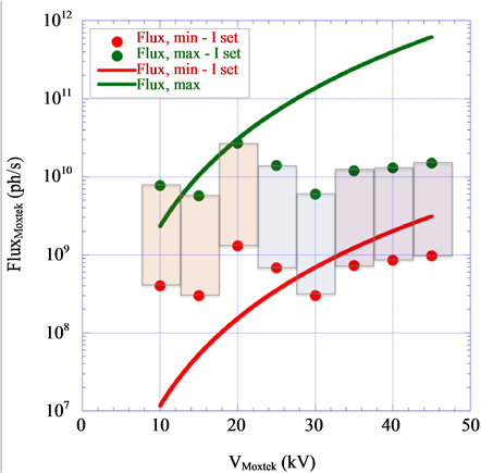
The calibration procedure of the Moxtek tube is given in Figure 1, where the results obtained from the first and final iteration steps are presented. In Figure 1, rectangles represent values between maximum and minimum measured flux at each high voltage step. The minimum (red curve) and maximum (green curve) flux, as obtained at the end of the calibration procedure, are shown. In Figure 1(a), a few rectangles fall outside of the range of emitted flux, as obtained at the end of the procedure, due to the uncertainties on the characteristics of filters and slits, air effects at the beginning of the procedure. Moreover, there is a lack of calibration omogenity in the range 10 - 50 kV, being the configurations very different each other. Configurations were gradually modified by eliminating the use of filters and trying to make them as homogenous as possible, for example same distance in air.

Table 1. Experimental configurations used to calibrate the SiPIN diode.
 (a)
(a)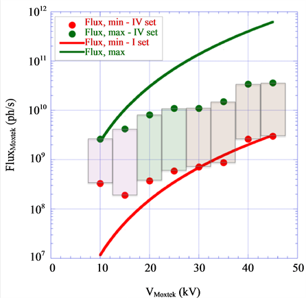 (b)
(b)
Figure 1. First (a) and last (b) set of measurements for Moxtek source calibration.
Final calibration cycle, Figure 1(b), was done with the Si-PIN diode at a distance (in air) from the detector of 300 mm and a slit, placed in front of the detector, having an active area of 0.1 mm2. The absolute minimum and maximum fluxes, emitted by the source, are then calculated based on this final calibration and shown respectively in red and green curves in Figure 1(a), Figure 1(b). Rectangles cannot cover all the possible interval of emitted fluxes, due to the limited dynamic range of the Si-PIN. Figure 1(b) is now considered as the final calibration of the Moxtek source in the range 10 - 50 kV, 1 - 200 μA, and will be used in the calibration of the detectors, as explained in the remainder of the Section.
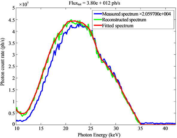
In Figure 2, the spectrum of the Moxtek source at 15 kV, acquired with Si-PIN diode located at 100 mm from the source and limited by a pinhole, is shown (blue line). The calculated spectral distribution at the exit of the source (Figure 2, green line) is obtained with Calib-X by including air absorption, solid angle, pinhole, detection efficiency of the Si-PIN and acquisition time. The correction of the air absorption causes a divergence at low energy and for this reason a cutoff at 4 keV is defined. The spectrum at the exit of the source is extrapolated linearly up to 0 keV and the effect of the Be window (250 μm thick) is then applied (Figure 2, red curve). Since the measured spectrum is 4 orders of magnitude less than the reconstructed spectra at the exit, it is multiplied by 2098 to be plotted in the same scale of the others. Moreover, the line at 5.9 keV is due to the Fe55 source, used in addition to calibrate the energy range. Pred-X was used to determine the spectrum detected by the SiPIN diode in the previous configuration (Figure 3, red curve) and it was compared with the measured spectrum (Figure 3, blue line) to debug the code, check its self-consistency and validate the extrapolation at low energy. In Figure 2 and Figure 3, the total flux emitted by the source at 15 kV - 50 μA (1.9 × 10⁹ ph/s) and detected with the Si-PIN diode (4.6 × 10³ ph/s) are also calculated, confirming that the flux emitted by the Moxtek tube is 105 - 106 times greater than the possible maximum flux acquired with Si-PIN diode.
In a similar way, the spectra for the Moxtek source at 45 kV are found with Calib-X and Pred-X and shown in Figure 4, Figure 5. In Figure 5, the agreement between simulated and measured response of Si-PIN diode is excellent. The Kα-line of Ag (21.9 and 22.1 keV) is evident in these spectra and it appears from 25 kV onwards.
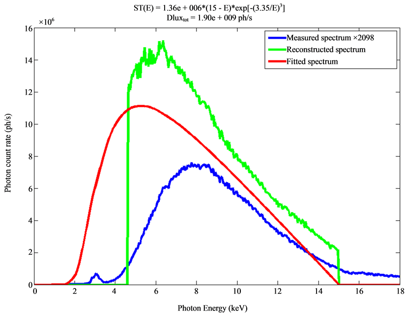
Figure 2. Acquired spectrum by a Si-PIN diode with the Moxtek source at 15 kV: measured (blue curve), reconstructed (green curve) and extrapolated spectrum (red curve).
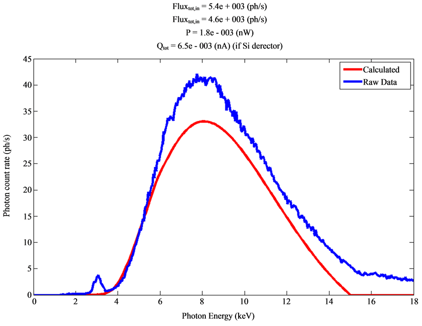
Figure 3. Comparison between the spectrum measured (blue curve) by Si-PIN diode and the simulated one (red curve) with the Moxtek source at 15 kV.
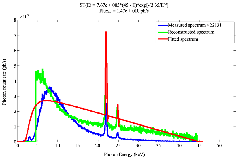
Figure 4. Acquired spectrum by a Si-PIN diode with the Moxtek source at 45 kV: measured (blue curve), reconstructed (green curve) and extrapolated spectrum (red curve).
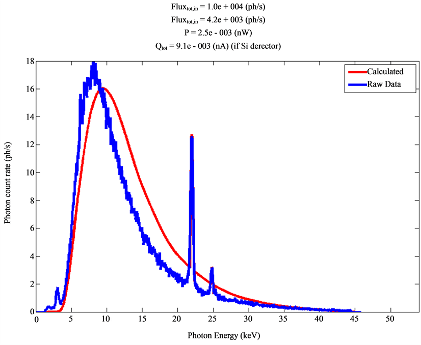
Figure 5. Comparison between the spectrum measured (blue curve) by Si-PIN diode and the simulated one (red curve) with the Moxtek source at 45 kV.
3. Cross Calibration of Different Sources and Detectors
In this Section the calibration of the other X-Ray source (Micro-focus tube) and detectors (SDD, low and high-energy range CdTe detectors) will be presented.
SDD spectrometer (Silicon Drift Detector) was calibrated, relying on the absolute flux emitted by the Moxtek tube. It has active area of 25 mm2, silicon thickness of 500 μm and energy resolution of 125 eV FWHM at 5.89 keV. The SDD is composed by two units: first, main detection unit composed by SDD module, preamplifier and mechanical cooling housing (XGL-SPCM-4110); second one, Power Supply, MCA and shaper unit (XGLMCSHPW-3110). The detection efficiency curve, Figure 6, was derived in the range 0 - 40 keV, thanks to the knowledge of the spectral flux of the Moxtek tube arriving on the detector. In addition, this curve was checked at low energy by using the Mo fluorescence L-line (2.3 keV) and the Fe55 source (5.9 keV), previously absolutely calibrated with the Si-PIN diode. The SDD detection efficiency at low energy is higher than the Si-PIN, due to a thin detector window and an higher absorption capability (500 μm Si thick) compared to Si-PIN diode.
A CdTe-based spectroscopic detector was also calibrated (AMPETEK X-123CdTe), having an active area of 9 mm2, a 1000 μm semiconductor thickness and a 100 μm Be window. It combines, in a single package, the CdTe drift X-ray detector and preamplifier, the digital pulse processor (AMPTEK DP5) and MCA, and the Power Supply (AMPTEK PC5). It requires only +5 VDC power and a standard communication interface. The detector is mounted on a thermoelectric cooler for reducing the electronic noise. It works in an energy range of 5 - 150 keV with energy resolution less than 1.2 keV FWHM at 122 keV and a count rates less than 2 × 10⁵. The CdTe spectroscopic detector was calibrated in energy with Mo fluorescence line (17.4 keV) and radioactive sources of Fe55 (5.9 keV) and BaCs (30 and 81 keV). The detection efficiency of CdTe detector (Figure 7) was found at low energy by means of fluorescence lines (5.9 and 17.4 keV), calibrated with Si-PIN, while at higher energy with the calibrated Moxtek spectra.
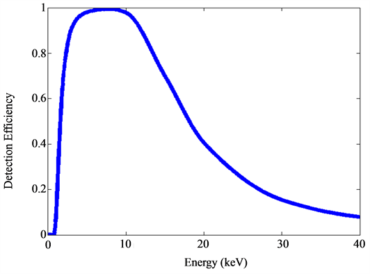
Figure 6. Derived detection efficiency of SDD detector as function of the energy.
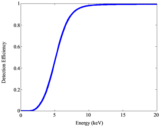
Figure 7. Detection efficiency of CdTe spectroscopic detector as function of the energy.
The CdTe spectroscopic detector covers the energy range up to 80 keV and it permits to calibrate the Micro-focus source (model Oxford Instruments SB-80-1M), as described next. The Micro-focus source is fully integrated, programmable, compact design, high voltage power supply and digital interface. It is characterized by having a tungsten anode, variable voltage in the range 35 - 80 kV and current in the 10 - 1000 μA, focal spot size of 33 μm. The spectra of the Micro-focus source were acquired with the CdTe spectrometer from 35 to 80 kV, with steps of 5 kV, and a distance from the source of 2500 mm (in air). The thick window of the tube produces a cutoff energy high enough to make negligible the air effect. Therefore the spectrum extrapolation at low energy was not required. In Figure 8 measured spectra (blue curves) and reconstructed ones (red curves) at 35 and 80 kV are shown.
Finally another CdTe detector (active area of 25 mm2, Be window thick of 254 μm, CdTe sensor 5000 μm thick), which ranges from about 30 keV to 1 MeV, was cross calibrated with the Micro-focus tube. The energy calibration was done with the BaCs radioactive source only.
Once the SXR sources were calibrated, transparencies of filters and effective areas of pinholes, currently used in the laboratory have been verified.
 (a)
(a)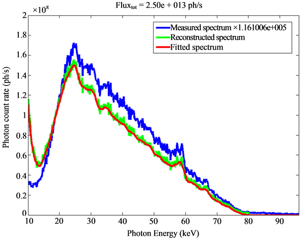 (b)
(b)
Figure 8. Acquired spectra with the CdTe spectroscopic detector and the X-ray Micro-focus source: measured (blue curves) and reconstructed (red curves): a) at 35 kV and b) at 80 kV.
The errors related to these calibrations of the X-ray tube emissivities are due to two contributions: one is relative to the uncertainties of the calibration curve of the Si-PIN diode, provided by manufacturer, and second one to the reconstruction methods, depending on parameters (air absorption, filters) known as theoretical curves. For the first contribution, the relative error is expected to be ±10%. Concerning the second, the following method has been adopted. Many spectra, in configurations different from those used for calibrations, have been simulated by changing air distance, filter thickness and geometry, and compared with the measured ones. The mean squared error and standard deviation σ, were calculated from each comparison, averaging over the energy range. The maximum error can be taken to be 3σ, giving a relative error of ±20%. Therefore, the total error on the calibration is expected to be ±30%.
 (a)
(a)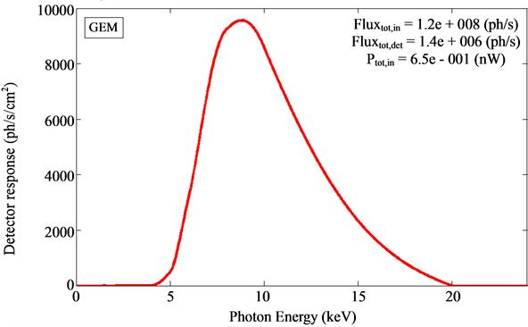 (b)
(b)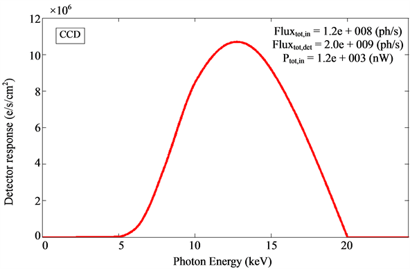 (c)
(c)
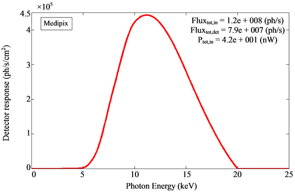
Figure 9. Simulations of the detector responses for Medipix-2 (a), GEM (b), CCD (c) with an X-ray source at 20 kV, 100 μA, 1 cm2, 0.1 mm Al filter and detectors at distance of 100 mm (in air).
4. Application to Gas and Solid State Imaging Detectors
The detection efficiency of X-ray imaging detectors, such as Medipix-2, GEM gas detector and CCD camera, were included in Pred-X to simulate the spectrum detected by these detectors. Pred-X computes also integrated values over the spectrum: the flux (ph/s) and the X-radiation power (nW) that arrives on the active area of the detector, the flux measured (ph/s) by the detector for devices working in photon counting (Medipix-2, GEM detector), the current generated (nA) for the detectors in current mode (SXR diodes) and the accumulated charges per pixel for CCDs.
The Medipix-2 photon counting chip, developed by INFN at CERN within the Medipix-2 Collaboration, is formed by a square matrix of 256 × 256 pixels, each of 55 × 55 μm2, resulting in an active area of 1.4 × 1.4 cm2. Each pixel of the semiconductor sensor (300 μm-thick Si) is bump-bonded to the corresponding channel of the chip (ASIC), providing analog and digital signal processing [5] . Detection efficiency of the Medipix-2 was estimated in the range 3 - 30 keV by utilizing the absolutely calibrated X-ray sources [6] .
The triple GEM detector is a micropatterned gas detector with three consecutive GEM foils, representing the amplification stages, and a 2D printed circuit board with 144 squared pixels. The detector has an active area of 10 × 10 cm2, while pixels have dimensions of 0.8 × 0.8 cm2 (12 × 12 squared pixels) [3] . The detector was characterized for two gas mixtures at atmospheric pressure: Ar/CO2 (70% - 30%) and Kr/CO2 (70% - 30%). The detection efficiency of the GEM detector was found in the range 2 - 30 keV for these two gas mixtures [7] .
The CCD camera (model Princeton Instruments PIXIS-XF1024F) is formed by a square matrix of 1024 × 1024, 13 × 13 μm2 pixels, resulting in an active area of 1.33 × 1.33 cm2 and it has a Beryllium window of 250 μm thick. The detection efficiency as function of the energy was found in the range 3 - 45 keV.
Finally, the prediction of the spectra acquired by different detectors (Medipix, GEM detector and CCD camera), in the case of a X-ray source at 20 kV, 100 μA, with 0.1 mm Al filter, an active area of 1 cm2 and a distance of 100 mm in air, are shown in Figure 9. The different spectral responses are due to the specific mechanisms for X-ray conversion and signal collection of the detectors.
5. Conclusion
A new X-ray Laboratory has been accomplished in ENEA-Frascati to develop X-ray diagnostics. X-ray sources, detectors, filters and the other optical components have been absolutely calibrated by means an innovative iterative method, developed on purpose, taking into account the difference (6 orders of magnitude) between the X-ray fluxes emitted by the sources and the measured ones by the spectroscopic detectors. More spectrometers have been required to cover the wide X-ray energy range 0 - 120 keV. Finally, thanks to these calibrations a predictive code (Pred-X) has been set up to estimate the absolute spectral distribution of X-ray photon flux in any experimental configuration. This is an extremely important tool for this laboratory to develop X-ray devices, and in particular for energy resolved detectors.
References
- Pacella, D., Romano, A., Gabellieri, L., Murtas, F. and Mazon, D. (2013) GEM Gas Detectors for Soft X-Ray Imaging in Fusion Devices with Neutron-Gamma Background. Nuclear Instruments and Methods in Physics Research Section A: Accelerators, Spectrometers, Detectors and Associated Equipment, 720, 53-57. http://dx.doi.org/10.1016/j.nima.2012.12.036
- Pacella, D., Dabagov, S., Murtas, F., Romano, A., Hampai, D., Gabellieri, L. and Mazon, D. (2011) Polycapillary Optics for Soft X-Ray Imaging and Tomography. IL NUOVO CIMENTO, 34, 513-520.
- Romano, A., Pacella, D., Mazon, D., Murtas, F., Malard, P., Gabellieri, L., Tilia, B., Piergotti, V. and Corradi, G. (2010) Characterization of a 2D Soft X-Ray Tomography Camera with Discrimination in Energy Band. Review of Scientific Instruments, 81, 10E523.
- Amptek. Efficiency Curves. http://www.amptek.com/xr100cr.html#efficiency
- Llopart, X., Campbell, M., Dinapoli, R., Segundo, D. and Pernigotti, E. (2002) Medipix 2: A 64-k Pixel Readout Chip with 55-μm Square Elements Working in Single Photon Counting Mode. IEEE Transactions on Nuclear Science, 49, 2279-2283. http://dx.doi.org/10.1109/TNS.2002.803788
- Gabellieri, L., Romano, A., Pacella, D., Causa, F., Murtas, F. and Claps, G. (2013) X-Ray Imaging in Tokamaks: Characterization of a C-MOS Imager (Medipix-2). Proceedings of the 40th EPS Conference on Plasma Physics, Espoo, 1-5 July 2013, 5-119.
- Pacella, D., Gabellieri, L., Romano, A., Causa, F., Murtas, F., Claps, G., Lee, S.H., Hong, J., Jang, J. and Choe, W. (2013) GEM-Based Energy Resolved X-Ray Tangential Imaging System on KSTAR. Proceedings of the 40th EPS Conference on Plasma Physics, Espoo, 1-5 July 2013, 5-118.