Journal of Electronics Cooling and Thermal Control
Vol.08 No.02(2018), Article ID:88883,12 pages
10.4236/jectc.2018.82002
Investigation and Comparison of the DIBL Parameter and Thermal Effects of SOD Transistors and SOI Transistors and Improving Them with the Change of Their BOX Thicknesses
Nooshien Laderian*, Arash Daghighi
Department of Engineering-Electronics Branch, Shahrekord University, Shahrekord, Iran

Copyright © 2018 by authors and Scientific Research Publishing Inc.
This work is licensed under the Creative Commons Attribution-NonCommercial International License (CC BY-NC 4.0).
http://creativecommons.org/licenses/by-nc/4.0/


Received: October 19, 2016; Accepted: June 26, 2018; Published: June 29, 2018
ABSTRACT
In this paper, thermal effects and Drain Induced barrier lowering (DIBL) of silicon-on-insulator (SOI) and silicon-on-diamond (SOD) transistors with 22 nm channel lengths using hydrodynamic simulations have been investigated. Thermal conductivity of diamond in contrast to thermal conductivity of silicon dioxide is significantly higher. Hence, the heat transfers faster in silicon-on-diamond transistors. Lattice temperature of SODs is lower than that of similar SOIs. By using SODs in Integrated circuits with the first transistor turning on and active, neighboring transistors will have the same level of heat as the active transistor. As a result, the DIBL factor will be increased; this is an undesired phenomenon in CMOS applications. To resolve this issue, we propose a new method which is the thickness reduction of buried diamond layers inside of transistors. Due to this change, DIBL of active transistor will be improved, the exceeding lattice heat of side transistors will be evacuated through the devices and their temperatures will be deduced in large scale.
Keywords:
Silicon-on-Diamond, Silicon-on-Insulator, Self-Heating, Off Current, DIBL

1. Introduction
Recently Silicon-on-insulator transistors have become a superior alternative for Bulk transistors. Their advantages over bulk transistors consist of: decreasing a link capacitor, short-channel effects improvements, leakage current reduction, latch up effects reductions, better noise reduction and many more advantages. SOIs have numerous applications such as: their usage in sensors, optical integrated circuits and micro electro-mechanical systems1. Their most demanding application is in integrated circuits design [1] . These semiconductor devices have a BOX layer within them which plays an important role in their electrical properties.
BOX layer in a silicon-on-insulator is filled with silicon-dioxide2. Silicon-dioxide has significantly small thermal conductivity (κ = 1.4 W/K-m) in comparison to other materials. The low thermal conductivity of the BOX layer results in self-heating effect and hence, it will make several unwanted problems. This phenomenon causes active current to decrease in the device, which in turn will reduce the carrier mobility and shift the threshold voltage of the transistor. The lifespan of the device will reduce as well [2] .
Great electrical insulating properties and also excellent thermal conductivity of diamond make it a superior substitute for silicon-dioxide in BOX region of SOI technology. Diamond despite of low thermal conductivity of silicon dioxide (κ = 1.4 w/k∙m) has high thermal conductivity (κ = 2000 w/k∙m). With the replacement of diamond, new types of transistors, called silicon-on-diamond transistors will be achieved. These transistors have the ability of transferring heat vertically to substrate and horizontally to contacts and connection points. By this act, the extra heat generated by the transistor can be evacuated [3] [4] . SOD device can be used as an alternative to standard SOI technology to eliminate the self-heating effect. Thus, the generated heat in the active silicon region of a SOD MOSFET will spread away from the junction into the underlying silicon substrate, die package and the heat sinks. This allows the application to operate in higher power levels as comparison to SOI MOSFET for the same junction temperature. Various experimental measurements demonstrate that SOD transistors can sustain more than 10 times higher power densities than the power densities withstand by SOI transistors [5] . With uniform transfer of heat, the heat is also unconsciously transferred to the neighboring transistors, and their temperature will rise. By this the off current of neighboring transistors will increase, in some cases even close to 8 times. Due to this change, compliance in analog integrated circuits that require high precision will be eliminated [6] [7] . Structure of SOD transistor is quite similar to the structure of SOI transistor with the exception of different material inside BOX region. Silicon-on-Diamond technologies, dependent on the thickness and impurity of channel region can be divided into two categories: Partially depleted SODs and Fully depleted SODs [8] .
The thermal conductivity is the parameter k in the Fourier expression for the heat flux:
(1)
q is amount of heat flowing per second and per unit area which is the heat flux and ∇T is the temperature gradient. The sign is chosen so that always k > 0, because of heat floatation from a high temperature to a low temperature
(2)
H is the amount of heat flowing per second through area A as a surface. Temperature gradient is , therefore:
(3)
If there are more layers applied, these equations can be extended:
(4)
These equations can be used for transistors with layers of different materials which have different thermal conductivities and different thicknesses [9] [10] .
The amount of heat transferred in any parts of semiconductor devices can be calculated and measured using the equations 1 - 4. In fact, we expressed equations 1 - 4 to explain that with regard to constant length, constant surface area and with the thermal conductivity k, the amount of heat transferred into any parts of device is related directly to the thermal conductivity of materials used. The greater the amount of thermal conductivity gets, the greater the amount of heat transferred into the device gets. With using materials with higher thermal conductivities such as diamond, the heat will transfer faster through the device and the undesirable heat will be evacuated quicker. By using SODs instead of SOIs, the problem of self-heating effect can be resolved.
Threshold voltage variation between low and high drain voltages is
called the DIBL parameter. Diamond has larger dielectric permittivity than silicon, because of larger dielectric constant of diamond rather than silicon dioxide. Consequently, the drain-body capacitance inside is also larger than the silicon dioxide. As a result, the drain effects the body and DIBL in SOD device is bigger than in SOI device [3] .
In this paper, lowering the diameter of BOX layer is proposed in order to improve DIBL parameter and also temperature of neighboring transistors in a SOD device. It is shown that due to this change, DIBL factor will reduce and also temperature of side transistors will decrease. The paper is organized as follows: the comparison of two devices are analyzed in Section 2, change in the structure of the device and simulation results are discussed in Section 3, followed by conclusion in Section 4.
2. Materials and Methods
Two device structures are chosen for further analysis: 1) SOI MOSFET, and 2) SOD MOSFET. The devices’ dimensions, parameters and structures are identical and taken from [2] . The transistor channel length is 22 nm.
Using hydrodynamic model for simulations, the accurate and reliable temperature profiles of the heat generated inside the transistors are obtained [10] . In hydrodynamic model, energy conservation equations for holes, electrons and lattice are solved simultaneously. Using this model, the temperatures of holes and electrons are not equal to the lattice temperature [9] . Models accounting for carrier mobility dependence on doping level, lattice temperature and band gap narrowing; Shockley-Reed-Hall recombination with concentration dependent lifetime; Auger recombination and temperature dependent saturation velocities and impact ionization coefficients are included. The default impact ionization coefficients are modified following the procedure mentioned in [11] .
3. Results
The intermediate results on SOI and SOD devices for the current drive and self-heating effects are presented here. Due to the higher temperature of SOI transistor in comparison to similar SOD transistor, the carrier mobility inside the active silicon layer decreases. For this reason, the drain current of SOI transistor is less than that of the similar SOD transistor. This means that by changing the buried insulating layer from silicon dioxide to diamond, temperature of the device decreases, and carrier mobility of SOD transistor becomes higher than the identical SOI technology. This is the reason why the drain current of SOD device is higher than the similar SOI device (Figure 1).
Figure 2(a) & Figure 2(b) shows the temperature profiles in both SOI and SOD technology. According to Figure 2, with bias voltage of 0.8 volts, lattice temperature of SOI in the body area is about 477 k and lattice temperature of body area of the similar SOD transistor is about 329 k. Temperature of buried

Figure 1. Id-Vd characteristics of SOI and SOD.
 (a)
(a) (b)
(b)
Figure 2. (a) Lattice temperature inside of the Silicon-on-Insulator device; (b) Lattice temperature inside of the Silicon-on-Diamond device.
layer of silicon dioxide in the SOI transistor is in the range of 350 k - 474 k and lattice temperature of diamond buried layer in SOD transistor is about 329 k.
Temperature of side transistors of SOD device increases to the same degree. This causes an increase in off current of neighboring transistors. In Figure 3, we made a cut through y-axis and see the active transistor’s lattice temperature of the device. Initial temperature of SOI device is 480 k, while according to the thermal conductivity of diamond, SOD technology creates a temperature of 330 k in the same conditions. Due to self-heating effect as well as the impact of thermal conductivity of diamond, unlike SOIs, in SODs, heat is distributed evenly through side transistors. The temperature difference is completely evident in Figure 4 and shows the effect of high thermal conductivity of Diamond.
In order to show the effect of Diamond layer instead of Silicon-dioxide layer in Box Region. Figure 4 shows the Lattice temperatures in 3D. An active SOI

Figure 3. Lattice temperature diagram of SOI and SOD, the view is through the y-axis.

Figure 4. 3D lattice temperatures of SOD and SOI.
transistor has a highest temperature of 480 k and the active SOD has the lower temperature of 330 k. The high thermal conductivity of Diamond layer causes the temperature to reduce dramatically and evacuates the undesired extra heat to the substrate and neighboring transistors. Now this question rises that if the temperature is increases in the neighboring transistors then what would be the solution for the problems caused by extra heat?
4. Discussion
The impact of heat generated in the active devices on the neighboring transistors in SOI and SOD substrates are discussed hereafter. For this reason, by adding 10 other transistors along each of the active SOI and SOD transistors, thermal effects of a working transistor on its neighboring devices are analyzed. Figure 5(a) & Figure 5(b) show the temperature distribution profiles of active SOD and SOI transistors in the same conditions. Lattice temperature in SOI technology because of low thermal conductivity of silicon dioxide, is not as uniform as SOD transistor. In SOI device, self-heating effect can be observed. The lattice temperature of neighboring transistors is less than that of side transistors of SOD device
 (a)
(a)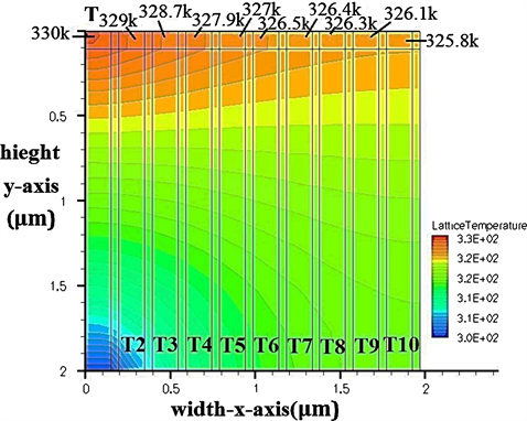 (b)
(b)
Figure 5. (a) Temperature distribution profile for SOIs. T is the active transistor; (b) Temperature distribution profile for SODs. T is the active transistor.
in the identical bias conditions. According to the temperature distribution profile of SOIs (Figure 5(a)), in a SOI the active region reaches the temperature of 480 k. In this case, a lot of heat generated in the active transistor transfer to the outside environment. Temperature of side transistors T2, T3, T4, T5, T6, T7, T8, T9, T10 respectively is 380 k, 360 k, 340 k, 330 k, 328 k, 326 k, 325.8 k, 324.7 k, 324.6 k. The initial temperature of transistors is 300 k. As a result of performance of active transistor, the temperature of each transistor respectively increases to 80 k, 60 k, 40 k, 30 k, 28 k, 26 k, 25.8 k, 24.7 k and 24.6 k. The active transistor transferees most of the heat to the T2 transistor.
According to the temperature distribution profile of SODs (Figure 5(b)), the temperature of the active region reaches 330 k. In this case also, some of the heat generated in the active transistor will be transmitted to the outside. Temperature of side transistors T2, T3, T4, T5, T6, T7, T8, T9, T10 respectively is about 329 k, 328.7 k, 327.9 k, 327 k, 326.4 k, 326.3 k, 326.1 k, 325.8 k. The basic temperature of these transistors is 300 k. As a result of active transistor performance the temperature of each transistor respectively increases to the 29 k, 28.7 k, 27.9 k, 27 k, 26.5 k, 26.4 k, 26.3 k, 26.1 k and 25.8 k. This uniform transfer of heat, causes the temperature of the channel region of the SOD transistor to be reduced more than that of SOI transistor.
Lattice temperatures of neighboring transistors of SOD active device are almost identical. This causes an increase in off-current of neighboring transistors. Lattice temperature variations of the SOI and SOD substrates along the X-axis at the exact same conditions are shown in Figure 6. Initial temperature of SOI

Figure 6. Lattice temperature diagram of SOI and SOD substrate along the x-axis with identical power consumptions, ISE TCAD simulations.
device is 480 k, while according to the thermal conductivity of diamond, SOD technology creates a temperature of 330 k at the same terms.
Figure 7 depicts the SOD substrate lattice temperature variation along the x-axis at the same junction temperature as SOI device. This junction temperature corresponds to 10-fold power density increase in SOD than SOI. As it can be seen, neighboring transistors in SOD substrate have much higher temperature than the temperature of the side transistors in SOI substrate. This increases the off-current and consequently increases the off-state power consumption of the devices. Therefore, thermal mismatch is a formidable task in high power density SOD applications incorporating thick diamond layer.
In order to investigate the impact of diamond layer thickness on thermal energy transfer to neighboring transistors, the thickness of the diamond layer is varied from 100 nm to 10 nm while retaining the identical junction temperature condition as SOI. The lattice temperature variations along the x-axis for various diamond layer thickness is depicted in Figure 8. As it can be seen, as the thickness of the diamond layer reduces, temperatures of neighboring transistors are sufficiently reduced. When the thickness of the diamond layer is 100 nm, the tail of the lattice temperature diagram is 447 k. When it is 60 nm, the tail of the lattice temperature diagram is 431 k and when the thickness is 40 nm, the lattice temperature becomes 423 k at the tail. By reducing the thickness down to 10 nm, the tail in lattice temperature diagram is 384 k. These results show that by decreasing the thickness of buried diamond layer, the heat energy transfer to the side transistors is decreased resulting in improved off-current characteristics and better thermal crosstalk immunity.

Figure 7. Lattice temperature diagrams of SOI and SOD substrates along the x-axis at the identical junction temperature. ISE TCAD simulations.
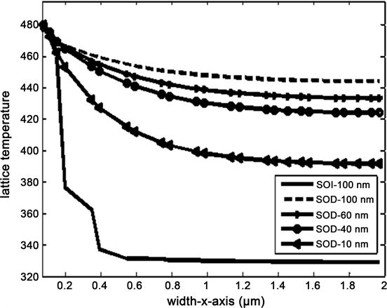
Figure 8. Lattice temperature diagrams for various diamond layer thicknesses along the x-axis with identical junction temperatures. From 100 nm to 10 nm thickness change, ISETCAD simulations.
Drain induced barrier lowering is a measure for short channel effects. For this reason, the DIBL variations of SOD and SOI transistors are also investigated. The DIBL of SOI device is 76 (mV/V) and DIBL of the identical SOD transistor is 82 (mV/V). The degraded DIBL in SOD device including thick diamond layer is the result of increased control of the drain on the body of the transistor through thick diamond layer. Therefore, reducing the thickness of the buried diamond layer lowers the fringing electric field that emanates from the drain and ends to the device body. Therefore, the impact of drain voltage on the device threshold voltage reduces.
By reducing the thickness of insulating oxide layer in SOI device and diamond layer in SOD transistor, the DIBL is calculated (Figure 9). As it can be seen, the DIBL of SOI device is 8% higher than that of SOD transistor at the insulating thickness of 100 nm. The amount of DIBL is proportional to the buried insulator thickness. When the thickness becomes 10 nm, both of the devices have identical DIBL values. Therefore, reducing the diamond layer thickness in SOD substrate, improves short channel effects.
5. Conclusion
Due to many advantages of SOIs over Bulk transistors they became a great alternative for Bulk devices in integrated circuits. The self-heating effect is an undesired phenomenon of these technologies; this issue can be solved by replacement of diamond instead of silicon dioxide in BOX region of the transistors. The
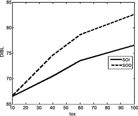
Figure 9. DIBL curves with comparison to oxide thickness variations, ISE TCAD simulations.
SODs have numerous advantages over SOIs; they can also withstand high power densities which will make them great candidates to be used in high frequency applications. In SOD devices by using a buried diamond layer due to the high thermal conductivity of diamond, heat uniformly transfers from the channel area to the substrate and to the neighboring transistors. This will reduce the temperature of the active transistor and at the same time, increase the lattice temperature of neighboring transistors. This heat transfer, occurs uniformly in diamond layer and in turn will increase the off current of side transistors at their temperatures which is an issue in integrated circuits. In order to reduce the off current of side transistors we can reduce the thickness of the diamond layer and by this change, temperature of neighboring transistors will be reduced. Thereby, the off current will be improved. Another issue regarding SODs is that their DIBL parameter is higher than the DIBL parameter of similar SOIs. This will cause a disturbance in the functionality efficiency of an integrated circuit. By reducing the thickness of diamond layer this problem will also be ruled out and the value of DIBL factor will be improved.
Conflicts of Interest
The authors declare no conflicts of interest regarding the publication of this paper.
Cite this paper
Laderian, N. and Daghighi, A. (2018) Investigation and Comparison of the DIBL Parameter and Thermal Effects of SOD Transistors and SOI Transistors and Improving Them with the Change of Their BOX Thicknesses. Journal of Electronics Cooling and Thermal Control, 8, 19-30. https://doi.org/10.4236/jectc.2018.82002
References
- 1. Colinge, J.P. (2004) Silicon-on-Insulator Technology: Materials to VLSI. 3rd Edition, Springer Science Business Media, New York, 1-360. https://doi.org/10.1007/978-1-4419-9106-5
- 2. Fiegna, C., Yang, E., Sangiorgi, A. and O’Neill, G. (2008) Analysis of Self-Heating Effects in Ultrathin-Body SOI MOSFETs by Device Simulation. IEEE Transactions on Electron Devices, 5, 233-244. https://doi.org/10.1109/TED.2007.911354
- 3. Daghighi, A. (2013) A Novel Structure to Improve DIBL in Fully-Depleted silicon-on-Diamond Substrate. Diamond & Related Materials, 40, 51-55. https://doi.org/10.1016/j.diamond.2013.10.010
- 4. Bresson, N., Cristoloveanu, S., Mazure, C., Letertre, F. and Iwai, H. (2005) Integration of Buried Insulators with High Thermal Conductivity in SOI MOSFETs: Thermal Properties and Short Channel Effects. Solid-State Electronics, 49, 1522-1528. https://doi.org/10.1016/j.sse.2005.07.015
- 5. Aleksov, A., Gobien, J.M., Li, X., Prater, J.T. and Sitar, Z. (2006) Silicon-on-Diamond—An Engineered Substrate for Electronic Applications. Diamond & Related Materials, 15, 248-253. https://doi.org/10.1016/j.diamond.2005.09.012
- 6. Rudenko, T., Nazarov, A., Kilchytska, V. and Flandre, D. (2016) A Review of Special Gate Coupling Effects in Long-Channel SOI MOSFETs with lightly Doped Ultra-Thin Bodies and Their Compact Analytical Modeling. Solid-State Electronics, 117, 66-76. https://doi.org/10.1016/j.sse.2015.11.017
- 7. Daghighi, A. and Zamani, S. (2009) Effects of 45 nm Silicon-on-Diamond Transistor. Majlesi Journal of Electrical Engineering, IV, 63-68.
- 8. Lukyanchikova, N., Garbar, N., Smolanka, A., Lokshin M., Simoena, E. and Claeysb, C. (2005) Origin of the Front-Back-Gate Coupling in Partially Depleted and Fully Depleted Silicon-on-Insulator Metal-Oxide-Semiconductor Field-Effect Transistors with Accumulated Back Gate. Journal of Applied Physics, 98, Article ID: 114506. https://doi.org/10.1063/1.2138380
- 9. Minnich, A.J., Dresselhaus, M.S., Ren, Z.F. and Chen, G. (2009) Bulk Nanostructured Thermoelectric Materials: Current Research and Future Prospects. Energy & Environmental Science, 2, 466-479. https://doi.org/10.1039/b822664b
- 10. Tritt, T.M. (2004) Thermal Conductivity, Theory, Properties, and Applications. Clemson University, Clemson, South Carolina, Kluwer Academic, Plenum Publishers, New York, Boston, Dordrecht, London, Moscow.
- 11. Dessis Manual, ISE Integrated System Engineering, Version 10,2004, Zürich, Switzerland.
NOTES
1MEMS.
2SiO2.