Optics and Photonics Journal
Vol. 3 No. 2A (2013) , Article ID: 33330 , 12 pages DOI:10.4236/opj.2013.32A001
Propagation and Confinement of Electric Field Waves along One-Dimensional Porous Silicon Hybrid Periodic/Quasiperiodic Structure
1Centro de Investigación en Energía, Universidad Nacional Autónoma de México, Temixco Morelos, México
2Física Teórica y Aplicada, Escuela de Ingeniería de Antioquia, Sede Las Palmas, Envigado Antioquia, Colombia
3Facultad de Ciencias, Universidad Autónoma del Estado de Morelos, Cuernavaca Morelos, México
Email: joesg@cie.unam.mx, memora@uaem.mx
Copyright © 2013 José Escorcia-García, Miguel Eduardo Mora-Ramos. This is an open access article distributed under the Creative Commons Attribution License, which permits unrestricted use, distribution, and reproduction in any medium, provided the original work is properly cited.
Received January 9, 2013; revised February 12, 2013; accepted February 19, 2013
Keywords: Optical Properties; Electric Field; Multilayers; Hybrid Structures
ABSTRACT
Selective spatial confinement of the electric field intensity is theoretically obtained for the light propagation along hybrid structures conformed by periodic and Fibonacci quasiperiodic dielectric multilayers. Sandwich-like configurations featuring periodic-quasiperiodic-periodic as well as quasiperiodic-periodic-quasiperiodic designs exhibit spatial localization of a large percent of the optical signal within specific zones of the hybrid system. Such a feature might be of interest in the pursuing of lasing devices based on porous silicon. It is found that the electric field confinement does not only depend on the quality of the defect or a particular transmission mode observed in the reflectivity spectra. We show that it is possible to enhance the electric field confinement solely varying the angle of incidence. The possibility of realizing finite photonic crystals with reduced size and very well defined band gap by means of a quasiperiodic-periodicquasiperiodic hybrid multilayer is also revealed.
1. Introduction
The engineering of electromagnetic modes at optical frequencies in artificial dielectric structures, with periodic, quasiperiodic or random variation in the refractive index, was first proposed independently by Yablonovitch, Kohmoto and John in 1987 [1-3]. Such kinds of complex dielectrics are often considered as photonic crystals or quasicrystals, and can be much easily obtained in a onedimensional multilayered configuration. Their attributes have generated worldwide research and development of sub-µm and µm size active and passive photonic devices such as a single-mode and non-classical sources, guided wave devices, resonant cavity detection, and components for optical communication.
Quasicrystals are non-periodic structures constructed following a simple deterministic generation. Among the different structural sequences used for quasicrystal fabrication one finds Cantor-like, Fibonacci (FN), generalized Fibonacci, Thue-Morse (TM), generalized ThueMorse, Period Doubling and Rudin-Shapiro. Although the FN system has been the subject of most study in this field. Electronic properties of FN multilayer structures are quite widely investigated (see for instance [4-7], and references therein). There are also studies on vibrational frequencies and atom displacements [8], as well as the propagation and localization of elastic waves [5,9-11]. Although less investigated than FN ones, the TM multilayered systems have also deserved significant attention. Their electronic properties have been studied, for instance, in [4,6,12,13]. In addition, some properties of elastic waves in quasiregular TM structures are reported in [14,15].
From the optical point of view, previously done work has focused on the study of the localization of light waves within FN quasiperiodic multilayer quasicrystals which leads to the appearance of photonic bandgaps, in a similar way to those existing in periodic structures. The photonic localization in the dielectric microstructure bears an analogy to the electronic localization in crystals [3]. Later on the concept of localization was recognized as applicable to any type of wave, such as acoustical wave [16]. Kohmoto et al. introduced the first system based on optical FN multilayers capable of localizing photons [2]. In 1994 Gellermann et al. showed experimental proof of the existence of bandgaps in the spectrum of FN dielectric multilayers [17]. There are also reports in the literature about the obtention of omnidirectional bandgaps using FN quasiperiodic structures [18,19]. A study on the features of the optical propagation in porous silicon-based FN polytype multilayers was put forward by Agarwal and Mora-Ramos [20]. Optical properties of non-Fibonacci 1D dielectric quasiregular systems have also been studied by some authors [20-41].
On the other hand, in a couple of works on quasiperiodic dielectric multilayers, E. Maciá outlined the possibility of designing hybrid dielectric heterostructures [42, 43]. Soon after, Wen et al. put forward the realization of an omnidirectional reflector made of on the basis of a Fibonacci-Bragg(periodic) hybrid system [44]. Then, for some years, the study of hybrid dielectric systems was practically out of literature. It is worth mentioning that during such period A. Montalbán and his collaborators lead a research on the behavior of oscillation modes in hybrid 1D periodic/quasiregular chains of point masses [45-47]. One of the main results of these works is the appearance of a selective spatial confinement of the vibration amplitudes, whether it is within the multilayered periodic part or whether it takes place within the quasiregular region of the structure.
Motivated by those reports on mechanical oscillations, in 2009 we presented some preliminary theoretical reports on the optical propagation in porous silicon-based multilayers designed as hybrid combinations of FN and Bragg mirror (BM) dielectric sections [48-50]. In these works we obtained an enhancement of in-gap microcavity mode localization as well as of the omnidirectionality of the reflectance properties of the structures proposed. Moreover, a significant selective spatial localization was detected for some propagating modes. That is, there are wavelengths for which the intensity of the electric field confines almost totally within the FN section or within a BM one. Some refinements of these results, but still preliminary ones were published in a more recent article [51]. It is worth mentioning that, later than the publication of our 2009 reports there have been some communications in relation with optical properties of hybrid periodic/ quasiregular and quasiregular/quasiregular hybrid dielectric heterostructures [52-54]. There is also a very recent experimental and theoretical report on tunable resonant transmission in a kind of porous silicon-based heterostructures [55]. The main interest in these works is focused on their use as reflectors and filters, and nothing is said there about the confinement or localization of the optical waves.
In this article we are aimed at developing a more detailed study of the selective spatial localization of the electric field of light waves propagating along hybrid FN-BM heterostructures. The discussion will consider both FN-BM-FN and BM-FN-BM multilayer designs together with the effects of the angle incidence and the variation of the dielectric contrast by changing the refractive index of the two basic layers involved. The work is organized with a section that follows on, presenting the model and the calculation scheme. Then there is a section containing the analysis and discussion of the obtained results. Finally, the main conclusions of the work shall be given.
2. Model and Methodology
A hybrid structure is defined as a combination of two independent structures with different properties, in this case a periodic and an aperiodic structure, to form a structure with superior features. As we previously mentioned, for the periodic part we choose the classical BM structure, while for the aperiodic we chose the FN one. These structures are produced with the use of the following substitution rules: Aj → Aj – 1Bj – 1, Bj → Aj – 1Bj – 1 and Aj → Aj – 1Bj – 1, Bj → Aj – 1 for the periodic and quasiperiodic structure, respectively. Both constituents have A0 = A and B0 = B as a seed. So, for instance, the third generation period structure is given by BM(3) = ABABABAB while the fourth generation Fibonacci structure is given by FN(4) = ABAABABA. Once they are constructed, the hybrid assembly design implies putting them together in a sandwich configuration, for which we are considering two different ways: BM-FN-BM and FN-BM-FN. In our particular case, we use the pair of refractive indices nA = 1.8 and nB = 1.2 which are commonly used in the fabrication of porous silicon heterostructures for photonic applications [20,34,36,39]. The choice for the layer widths is made according the quarter-λ rule: dA,B = λ0/4nA,B, with λ0 = 800 nm. The Figure 1 schematically shows the BM-FN-BM design, with the indication of the incident, reflected and transmitted waves. Viewed in this way, the proposed structure can be considered as a system of two or more defects (depending upon the particular order of the FN generation) included in the otherwise periodic configuration. A bulky defect would be obtained if the central (FN) part were made of layers with values of the refractive index distinct to those used in the BM part. But this possibility will not be discussed here, rather it could be the subject of another study.
The calculation of the electric field of s and p polarizations in the hybrid dielectric multilayer uses the well known transfer matrix method. Its details can be found elsewhere [56-58]. The approach makes provision for the variation of the angle of incidence as well as for the discontinuity in the dielectric properties when passing from a layer A to a layer B and viceversa. Within this framework, we are able to calculate the reflection and transmission coefficients, but our main interest is the obtention of the relative electric field intensity (defined as the quotient |E(z,ω)/Ei|2, with Ei being the amplitude of the incident signal) as a function of the position z in the structure, measured from the point of light incidence. The expression that allows us to evaluate the electric field amplitude in terms of the transfer matrix is

where wαβ are the elements of the matrix that connects the field at the extreme left-hand interface with the layer in which the coordinate z lies. The quantity r(ω) is the complex reflectance of the whole structure, and the factor γ0 appears as a result of the imposition of suitable boundary conditions on the field components at the interface of light incidence (see Figure 1). Then, the field intensity is simply the absolute square of the electric field, |E|2, which is normalized to the amplitude of the incident wave.
3. Results
The Figure 2 contains the calculated optical properties of hybrid Bragg-Fibonacci heterostructures in different configurations. The color density graphics correspond to the relative electric field intensity associated to the optical mode with energy hω (vertical axis), at a given position z in the multilayer structure. On the side insets, one can see the corresponding normal-incidence reflectance, R = |r(ω)|2, in each case.
In the graphics 2a and 2b we are representing the results for hybrid BM3-FN4-BM3, and aBM3-aFN4-aBM3 dielectric heterolayers. The prefix “a” indicates that the structure considered has the refractive indices of its layers
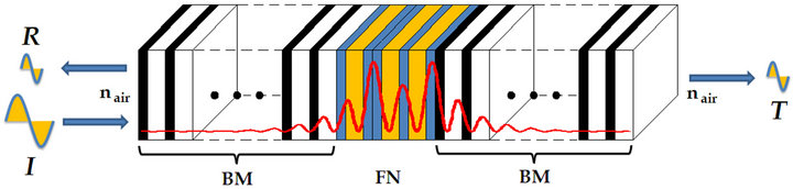
Figure 1. (color online) Schematic representation of the incidence and propagation of the electric field wave along a hybrid BM-FN-BM.
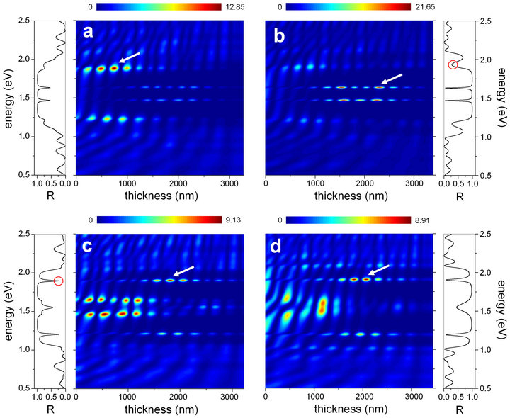
Figure 2. (color online) Distribution of the relative electric field intensity along the hybrid structures for (a) BM3-FN4-BM3, (b) aBM3-aFN4-aBM3, (c) FN4-BM3-FN4, and (d) aFN4-aBM3-aFN4 with the positions of the corresponding |E|2 maxima whose values appear at the right of the color bars over the figures, indicated by arrows. The insets on the side of each graph gives the reflectivity at normal incidence of the particular structure.
exchanged; that is, nA ↔ nB. Both BM3 and FN4 parts consist of eight monolayers. On the other hand, the FN4 contains a total of five “A” layers whilst there are only four in the BM3. This makes the physical thickness of each part to have a different value. According to the λ/4 design, the BM3 and aBM3 parts have the same width: 1111 nm. However, the total thicknesses of the FN4 and aFN4 substructures are different: 1056 nm and 1167 nm, respectively. Color bars located above each graphics serve as intensity-scale indicators: from zero (deep blue) at the left to maximum (dark red) intensities at the right. In each case, the maximum value of the relative intensity attained within the structures appears at the top right of the figure. The arrows are pointing at the positions of such maximum intensity peaks within the structures.
From the analysis of Figures 2(a) and 2(b) we can see that the relative field intensity of some particular modes show a selective spatial confinement, whereas the intensity of the electric field of the remaining propagating optical modes in the energy interval considered distributes rather homogeneously throughout the structure, with the normal occurrence of maxima and minima resulting from the multiple interference. Of course, the far lefthand part of the system shows the presence of illuminated zones even in the energy region within the photonic band gap. This is due precisely to its proximity to the surface of light incidence. The maximum relative intensity of the BM3-FN4-BM3 corresponds to a mode with energy immediately above the gap. The most of the spatial location of the associated electric field squared amplitude is approximately at the middle point of the left Bragg mirror. One readily sees that when z > 1000 nm, the relative intensity decreases significantly. It is possible to observe also the spatial localization of rather high field intensity in the left-hand Bragg multilayer. The energy of such a mode is now immediately below the gap. However the values of |E|2 in this case are smaller. For these two optical modes, the confinement of a greater part of the electric field amplitude at the left of the system can be explained as follows: The remaining parts of the hybrid heterostructure are acting as mirrors that reflect the light back to the left (notice that the region containing the right-hand Bragg part is colored in darker blue which means that almost no light is propagating throughout it).
There are two signals of low, but nonzero relative intensity with spatial field localization mainly in the central FN4 substructure. These correspond to the pair of microcavity modes within the photonic band gap. Such modes can be related with the situation of a “double A-defect”, introduced by the FN substructure. The same double microcavity is present in the aBM3-aFN4-aBM3 configuration Figure 2(b). They are at the same energy position of those of the BM3-FN4-BM3 structure; but from the reflection spectrum one may see that they are sharply defined, reaching almost the unity transmission. With regard to their spatial field dependence, we can say that the change in the dielectric contrast (with nA now having the lower of the two values) has led to the change in the relative intensity localization. In this case the microcavity modes and not the bandgap-edge ones exhibit the strongest confinement, which takes place within the aFN4 region this time.
Figures 2(c) and 2(d) show the calculated relative intensity and total reflectance for hybrid FN4-BM3-FN4 and aFN4-aBM3-aFN4 multiple heterolayers. This is not the typical Bragg-microcavity optical complex design. Now the photonic band gap appears split into two parts separated by a region containing two main propagating modes, whose relative intensities confined mostly within the left-hand FN4 or aFN4 substructures. Interestingly, the process of multiple internal reflections in the hybrid system makes these two optical signals to travel along the structure in such a way that, close to its right-hand end, they seem to merge into a wave with a an intermediate frequency. This frequency is the one at which there is a local minimum of the reflectance in the separated transmission gap structure.
However, the highest relative field intensity in these structures corresponds to a microcavity-like mode located close to the high-frequency edge of the photonic band gap. In this case, the main spatial confinement of the field occurs in the central BM part of the hybrid multilayer, although non-vanishing field intensities can be observed in the two adjacent FN4 substructures as well. In all, the highest values of the relative intensities attained at the maxima indicated by the arrows, are smaller than those occurring in the BM3-FM4-BM3 structures of Figures 2(a) and 2(b).
The physical reason behind the behavior of the light propagation in the hybrid dielectric heterostructures is the process of multiple internal reflections associated to the interfaces that separate regions of different dielectric properties. The discussion made above assumes that the light incidence to be normal to the layers. However, the electromagnetic usually reaches the structure forming an angle with the normal to the layer’s plane. Then, there will be multiple Snell-type refraction processes at the interfaces. Taking this into account, the Figure 3 presents the spatial distribution of the calculated relative field intensity for particular optical modes as a function of the angle of incidence.
Figure 3(a) contains the relative field intensity of both the s and p polarizations of an optical wave signal with a frequency mode of 1.8955 eV propagating in the FN4- BM3-FN4 hybrid dielectric heterostructure considered above. In the case of the p polarization, the field intensity distributes rather homogeneously over all the spatial
 (a)
(a)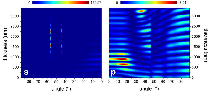 (b)
(b)
Figure 3. (color online) Dependence of the relative electric field intensity as a function of the incidence angle, for both s and p mode polarizations, in the structures (a) FN4-BM3-FN4 and (b) aBM3-aFN4-aBM3. The particular mode considered corresponds to the photon energies of 1.8955 eV and 1.9335 eV, respectively. These energy positions are indicated by a red circle in the reflectance spectra of each structure in Figure 2.
extension of the system for angles of incidence above 50˚, whilst for angles between 40˚ and 50˚ there is tendency of a larger spatial confinement within the left hand FN4 multilayer; but with no particularly significant values of the intensity (see the corresponding color bar above). In the angular region extending approximately between 20˚ and 40˚, the propagation is very much reduced, with only a small portion of the field penetrating the left FN4 and almost zero intensity in the sandwiched BM3 substructure and the right FN4 portion. The most interesting results regarding the selective spatial localization of the wave field correspond to the interval of oblique incidence with angles between 0 and 10 degrees. Here, the relative field intensity strongly localizes within the BM3 substructure, with the maximum equals to the reported in Figure 2(c) for normal incidence; but with the feature that this spatial confinement is kept even for a light incidence with up to 8˚.
The s polarization wave for this specific mode shows the same spatial localization within the central BM3 substructure, as compared for p, for angles of incidence between 0 and 8 degrees, approximately. Oblique angles between 8˚ and 48˚, and above 70˚ for the light incidence lead to almost zero propagation of the s signal in the entire structure. However, there two narrow angular fringes, centered at ~50˚ and ~68˚ for which we can observed a strong spatial confinement of the field amplitude within the left FN4 multilayer with separated bright spots having relative intensities above 10, which surpasses the normal incidence highest value in this heterostructure. Again, for angles between those two narrow fringes, the field barely propagates along the hybrid dielectric system.
In the Figure 3(b), the results for the dependence of the relative intensity on the angle of oblique incidence correspond to a hybrid aBM3-aFN4-aBM3 structure. In this case, the signal with p-type polarization also displays a rather extended intensity distribution over the entire system for all angles of incidence considered. The maxima of the relative field amplitude confine mostly within the first aBM3 substructure when the angle are between zero and 25˚ approximately. The highest one appears at about 900 nm from the interface of light incidence and corresponds to a value of 8.04, which is slightly bigger than its value obtained at normal incidence.
The situation for the s-type polarization wave is drastically different in this hybrid heterostructure. As we can readily observe, the propagation of this optical signal throughout such a dielectric multilayer is almost entirely forbidden. The relative field intensity shows very small values in the first half of the structure length, for angles between 0˚ and 10˚. The signal barely travels inside the system for angles larger than 30˚, with the exception of two very narrow angular fringes approximately centered at 44˚ and 57˚. For these angles the s-wave propagates along the entire dielectric heterostructure and the relative field intensity is largely localized within the central Fibonacci substructure. It is a significant fact that the oblique incidence of ~57˚ boosts the localized intensity corresponding to this field polarization to relative values as high as 122.57.
To complement the discussion above, the Figure 4 shows the calculated relative intensity maps and the reflectance spectra for the FN4-BM3-FN4 (Figure 4(a)) and the aBM3-aFN4-aBM3 (Figure 4(b)) hybrid systems. In these cases, a finer angular partition allows to detect the oblique incidence that leads to the largest values of the spatially localized relative s-field intensity. For the hybrid FN4-BM3-FN4 structure, the maximum value is equals to 17.43 and is reached at 69.2 degrees of incident light ray inclination with respect to the first FN4 interface. On the other hand, the value of the maximum |E|2 is obtained, in the case of the aBM3-aFN4-aBM3 heterostructure, when the propagation wavevector of the incident ray forms an angle of 58.2 degrees with respect to the normal direction to the leftmost aBM3 surface (see the diagram of Figure 1 for reference. Such a value is notably of 137.59. The field intensity in the FN4- BM3-FN4 multilayer shows a selective spatial localization which is mostly confined within the left-hand FN4 substructure. However, the spatial confinement of the optical wave in the aBM3-aFN4-aBM3 structure takes place mainly within the central fourth-generation Fibonacci layered region.
It is worth analyzing the information provided by the calculated reflectance spectra included in Figures 4(a) and 4(b). In the case of the FN4-BM3-FN4 hybrid heterostructure, we can observe a wide photonic band gap for energies above 1.3 eV. Within this gap there are two microcavity propagating modes whose energies are slightly below 1.5 eV and 2.0 eV, respectively. Such a wide gap, obtained for an incidence of 69.2˚ indicates the prospec-
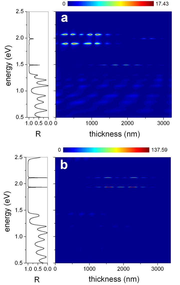
Figure 4. (color online) Enhancement of the confinement of the |E|2 intensity for the structures (a) FN4-BM3-FN4 and (b) aBM3-aFN4-aBM3, showed in the Figure 2, at the following incidence angles of 69.2˚ and 58.2˚, respectively.
tive usefulness of hybrid heterostructures as omnidirectional mirrors, as it was proposed in reference [51]. The waves that exhibit selective spatial confinement at this particular angle of incidence are not propagating modes but modes with zero transmission. Due to the combined reflecting effects of the Bragg and right-hand Fibonacci multilayers, these waves undergo a process of multiple interferences that leads to the enhancement of the electric field amplitudes within the left part of the structure.
The reflectance spectrum appearing in the Figures 4(b) (case of the aBM3-aFN4-aBM3 hybrid multilayer) also shows a rather wide photonic band gap extending from slightly below 1.5 eV up to a photon energy of approximately 2.4 eV, when the incidence angle is of 58.2˚. For this structure, the modes that show selective spatial confinement of the field intensity are the microcavity modes on both sides of the 2.0 eV, which do propagate throughout the entire structure (notice that transmittance is equals to unity for them). The relative field intensity achieves a large value for its maximum, and is confined mostly within the central FN substructure.
Then, according to the information contained in Figures 3 and 4, it can be established that the variation of the angle of incidence of the incoming electromagnetic wave may be used for tuning the presence of a significant selective spatial confinement of the field radiation intensity within hybrid Bragg-Fibonacci dielectric heterostructures.
We must highlight that the results discussed up to this point are related with structures that have a relatively low number of constituent layers (the BM3-FN4-BM3 has 24). It is possible that this number can be reduced by using materials with a different dielectric contrast, and the outcome would be similar. To analyze the influence of the augment in the number of dielectric layers in the system, Figure 5 contains the calculated relative field intensity for normal incidence in four aBM-aFN-aBM hybrid heterostructures. The order of the central Fibonacci multilayer is kept fixed as fifth. Then, the order of the Bragg-type sandwiching substructures varies from second Figure 5(a) to fifth Figure 5(d). In the four cases, the highest values of the relative field intensity correspond to signals with amplitudes confined within the FN part. But, as can be readily seen, the maximum amplitudes and their energy positions are quite different from one case to another. For instance, the propagating optical signals that show the greater spatial intensity localization in Figures 5(a) and 5(b) correspond to the three microcavity-like modes associated to the three “A-defects” of the FN5 substructure (AB-AA-BAB-AA-B-AA-B in detail). Whereas, the multilayers with higher orders of the Bragg periodic sequence Figures 5(c) and 5(d) have the spatially localized signal corresponding to a single energy, which is the one corresponding to the lowest of the three confined modes detected in the structures with the lower BM orders. In this sense, for the set of dielectric parameters chosen in the study, the increase in the number of Bragg mirrors makes the entire system to behave as if it were to include a single microcavity-like defect. If we compare the maximum values of the relative field intensities achieved in the case of Figure 5(c), it seems like the effects of the three optical defects in the central region merge in such a way that the amplitude of the confined radiation enhances given a maximum value |E|2 equals to ~462. A further augment in one order of the BM generation keeps a stronger localized single-microcavity-like relative intensity, but the maximum value achieved reduces to ~150. What is happening
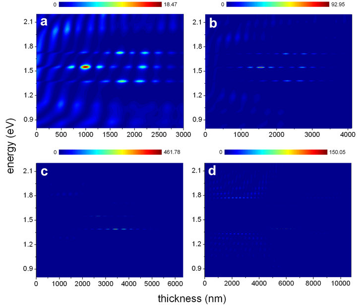
Figure 5. (color online) The relative field intensity of optical modes in a hybrid aBM-aFN-aBM dielectric multilayer as a function of the position in the structure. The order of the central Fibonacci sequence is kept fixed as fifth. The order of the sandwiching BM binary heterolayers varies as following: (a) aBM2; (b) aBM3; (c) aBM4; (d) aBM5.
here is that there is a redistribution of the wave field and a substantial part of it confines now within the left-hand BM substructure or simply reflects from the system. A small part of the signal, corresponding to the BM photonic band gap edges, propagates throughout the structure.
The field intensity distribution of the type detected within the higher-order BM substructure in Figure 5(d) can be much better observed if we construct a hybrid aFN-aBM5-aFN hybrid multilayer. The Figure 6 shows the results for the calculated relative electric field intensity as a function of the position in the heterostructure. In this situation, the orders of the Fibonacci sequences used to design the sandwiching FN parts rank from third Figure 6(a) to sixth Figure 6(d).
The general appearance in these four graphics is that of a very well defined BM-related photonic band gap with a direct space picture of allowed and forbidden optical modes of propagation. In the structure possessing the largest FN order Figure 6(d), the BM photonic gap remains but the influence of the more disordered FN multilayers destroys the regular arrangement of light intensities above and below the gap displayed in Figures 6(a)-6(c). Also, the largest confined intensities (within the BM part) in this case correspond to a mode with energy above the BM photonic gap (with the higher value of ~112), whilst in the three other cases Figures 6(a)-(c) the maxima correspond to a band gap edge mode.
The BM-related regular distribution of lit and dark fringes in the energy scale is better noticed from the results obtained for the aFN4-aBM5-aFN4 and aFN5- aBM5-aFN5 systems, compared with the hybrid aFN3- aBM5-aFN3. In the cases of FN4 and FN5 components, the allowed modes propagate to a lesser extent within the right-hand FN substructure. Nonetheless, in all the four cases studied, one may observe that the light penetrates largely inside the left-hand FN multilayer, with energies that are within the BM photonic gap. Then, as soon as the waves with those frequencies reach the Bragg central part, they are reflected back.
With the same FN5 sandwiching multilayers, the rise of the order of generation of the central Bragg mirror region leads to the reestablishment of the BM-related field intensity distribution of allowed and forbidden mode intensities discussed above. This can be seen from the Figure 7, in which we are presenting the calculated |E|2 for an aFN5-aBM6-aFN5 hybrid heterostructure. In addition, the two profiles of the relative field intensity as a function of the position for the band edge modes are shown. From them, the selective spatial localization of the wave field, as well as the enhancement of the optical intensity are readily seen.

Figure 6. (color online) Distribution of the electric field along the hybrid structures for: (a) aFN3-aBM5-aFN3; (b) aFN4-aBM5-aFN4; (c) aFN5-aBM5-aFN5; (d) aFN6-aBM5-aFN6.
By observing the regular layout of dark and lit frequency regions along the vertical axis of the field intensity distribution in Figures 6 and 7, it is apparent that the design of hybrid FN-BM-FN dielectric heterolayers brings forward the possibility of the practical realization of finite and reduced size photonic crystal systems with a well-defined structure of allowed and forbidden propagation fringes. Besides the selective spatial localization of the wave field intensities, these heterostructures can act simultaneously as optical filters for several intervals of the radiation energy, other than the fundamental gap. We readily notice that the photonic band is an intrinsic feature of the Bragg mirror part of the structure, which is kept independently of the order of the Fibonacci generation corresponding to the outer substructures. Of course, the better design of these photonic systems would be a compromise between the orders of the periodic and quasiperiodic multilayers, the values of the refractive indices and the layer widths, mainly. Our experience performing numerical simulations with these hybrid structures is, for instance, that the increase of the order of the FN part beyond the fifth in a system like the one used to obtain the Figure 7 may lead to an important growth in the maximum of the relative field intensity localized within the central BM region. However, the distribution of allowed and forbidden energies practically does not change with respect to that shown in the figure.
At this point, it is necessary to briefly comment some possible restrictions to the results presented here. They are associated with the influence of factors that were not included in the model. The calculation performed in this work has assumed ideal conditions such as perfect flat interfaces and no absorption losses. It is clear that interface roughness may lead to reduced reflectance and narrower photonic band gaps given the scattering of the light rays away from the direction of propagation. This was discussed in [20]. In addition, the travel of an optical signal through a real porous silicon-based hybrid heterostructure would suffer from the Rayleigh scattering associated to the intrinsic structural disorder of a porous material, as it was shown in reference [59]. On the other hand, the optical absorption phenomenon would be responsible for a reduction of the optical intensity, thus affecting the values of |E|2. However, in the case of porous silicon structures, the light absorption takes place mainly for frequencies in the visible blue range and above, whilst at wavelengths around our λ0 = 800 nm, the absorption losses are less significant. Despite the possible quantitative modifications that our results might suffer due to these limiting effects, the essence and main qualitative features of the spatial light localization should be kept in a real hybrid structure. Arguments in favor of this conclusion can be found in the satisfactory agreement found in comparisons between theoretical and experimental optical properties of porous silicon quasiregular multilayers published in recent years [32,34,36, 37,39].
4. Conclusions
In this work we have presented a theoretical investigation of the light propagation on hybrid Fibonacci-Periodic dielectric heterostructures. The main purpose of the study

Figure 7. (color online) Distribution of the electric field along the hybrid structures aFN5-aBM6-aFN5 showing a maximum of |E|2 equals to 124.24. The energies of the two particular modes represented correspond to the upper and lower photonic band gap edges.
was to show the possibility of selective spatial confinement of the optical field intensity within this kind of systems. The results of our calculation reveal that both Periodic-Quasiperiodic-Periodic and Quasiperiodic-Periodic-Quasiperiodic configurations can be used to achieve such a spatial confinement of the light field. In some cases, it is shown that high values of the relative intensity can be obtained in hybrid multilayers made from a quite small number of dielectric layers. Additionally, we have obtained that the variation in the angle of light incidence can be a suitable tool for tuning larger values of the confined field intensity. The calculation has been performed using values of the refractive indices typical of the porous silicon. We believe that the use of constituent materials showing higher dielectric contrast will allow achieve higher values of the confined electric field intensity in hybrid heterostructures. The choice made here for the indices of refraction pursues the possibility of practical realization of this kind of systems via the growth of porous silicon multilayers. That is a cheap procedure by which it is possible the controlled obtention of dielectric layers with n varying from slightly above the unity to 2.5, with layers widths starting from around 7 - 8 tens of nanometers.
Our numerical simulations reveal the possibility of designing multilayer-based photonic crystals with a well defined structure of allowed and forbidden frequencies for the light propagation, using hybrid Fibonacci-BraggFibonacci heterostructures. Given their finite and reduced size, these systems might be of interest for the fabrication of optical devices. In addition, the prediction of the selective spatial localization of some photonic modes, with rather high relative intensity confinement might result of interest in researches looking for plausible lasing regimes using porous silicon dielectric multilayers.
It is worth mentioning that, in order to illustrate the introduction of a hybrid design in the investigation of the spatial mode localization in porous silicon-based onedimensional photonic system, our work has dealt with Bragg-Fibonacci multilayer structures that only involve lower FN or Bragg generations. This is mainly done for the sake of simplicity. Because no previous studies on the subject seem to have been published so far, our goal here was above all to discuss with some extent some physical properties related with the spatial localization of the modes that propagate in the structures. Besides, we choose the simplest configuration, in which “defect-like” layers are made of the same materials that form the layers considered as periodic or quasiregular “mirrors”. In consequence, the results for the spatial localization of the amplitude of the electromagnetic wave can also outcome from a usual “microcavity” theory. However, the use of distinct dielectric configurations in Bragg and quasiregular subsystems (as it was done in [55]), the incorporation of another aperiodic sequences (Thue-Morse, RudinShapiro, etc.), and different geometries (varying the number and widths of the layers) may lead to even more appealing possibilities of application for these heterostructures.
5. Acknowledgements
MEMR thanks hospitality from Escuela de Ingeniería de Antioquia for a sabbatical stay. He acknowledges Mexican CONACYT for support through grants CB-2008 No. 101777, and No. 180636.
REFERENCES
- E. Yablonovitch, “Inhibited Spontaneous Emission in Solid-State Physics and Electronics,” Physical Review Letters Vol. 58, No. 20, 1987, pp. 2059-2062. doi:10.1103/PhysRevLett.58.2059
- M. Kohmoto, B. Sutherland and K.Iguchi, “Localization of Optics: Quasiperiodic Media,” Physical Review Letters, Vol. 58, No. 23, 1987, pp. 2436-2438. doi:10.1103/PhysRevLett.58.2436
- S. John, “Strong Localization of Photons in Certain Disordered Dielectric Superlattices,” Physical Review Letters, Vol. 58, No. 23, 1987, pp. 2486-2489. doi:10.1103/PhysRevLett.58.2486
- R. Perez-Alvarez and F. Garcia-Moliner, “Some Contemporary Problems in Condensed Matter Physics,” Nova Science, New York, 2001, pp. 1-37.
- R. Perez-Alvarez, F. Garcia-Moliner and V. R. Velasco, “Some Elementary Questions in the Theory of Quasiperiodic Heterostructures,” Journal of Physics: Condensed Matter, Vol. 13, No. 15, 2001, p. 3689. doi:10.1088/0953-8984/13/15/312
- J. E. Zarate and V. R. Velasco, “Electronic Properties of Quasiperiodic Heterostructures,” Physical Review B, Vol. 65, No. 4, 2001, Article ID: 045304. doi:10.1103/PhysRevB.65.045304
- V. R. Velasco and F. Garcia-Moliner, “Electronic Spectra of Quasi-regular Heterostructures: Simple versus Realistic,” Progress in Surface Science, Vol. 74, No. 1-8, 2003, pp. 343-355. doi:10.1016/j.progsurf.2003.08.027
- E. Maciá and F. Domínguez-Adame, “Electrons, Phonons and Excitons in Low Dimensional Aperiodic Systems,” Editorial Complutense, Madrid, 2000.
- V. R. Velasco, R. Pérez-Alvarez and F. García-Moliner, “Some Properties of the Elastic Waves in Quasiregular Heterostructures,” Journal of Physics: Condensed Matter, Vol. 14, No. 24, 2002, p. 5933. doi:10.1088/0953-8984/14/24/305
- H. Aynaou, E. H. El Boudouti, B. Djafari-Rouhani, A. Akjouj and V. R. Velasco, “Propagation and Localization of Acoustic Waves in Fibonacci Phononic Circuits,” Journal of Physics: Condensed Matter, Vol. 17, 2005, p. 4245.doi:10.1088/0953-8984/17/27/002
- H. Aynaou, A. Nougaoui, E. H. El Boudouti, D. Bria, V. R. Velasco and B. Djafari-Rouhani, “Comparative Study of the Sagittal Elastic Waves in Metallic and Semiconductor Multilayer Systems between Period and Fibonacci Superlattices,” Surface Science, Vol. 584, No. 2-3, 2005, pp. 199-213. doi:10.1016/j.susc.2005.03.057
- C. S. Ryu, G. Y. Oh and M. H. Lee, “Extended and Critical Wave Functions in a Thue-Morse Chain,” Physical Review B, Vol. 46, No. 9, 1992, pp. 5162-5168. doi:10.1103/PhysRevB.46.5162
- C. S. Ryu, G. Y. Oh and M. H. Lee, “Electronic Properties of a Tight-Binding and a Kronig-Penney Model of the The-Morse Chain,” Physical Review B, Vol. 48, No. 1, 1993, pp. 132-141. doi:10.1103/PhysRevB.48.132
- V. R. Velasco, J. E. Zárate, “Elastic Waves in Quasiperiodic Structures,” Progress in Surface Science, Vol. 67, No. 1-8, 2001, pp. 383-402. doi:10.1016/S0079-6816(01)00038-7
- J. Tutor and V. R. Velasco, “Some Properties of the Transverse Elastic Waves in Quasiperiodic Structures,” International Journal of Modern Physics B, Vol. 15, No. 21, 2001, pp. 2925-2934. doi:10.1142/S0217979201007129
- S. He and J. D. Maynard, “Detailed Measurements of Ineslatic Scattering in Anderson Localization,” Physical Review Letters, Vol. 57, No. 25, 1986, pp. 3171-3174. doi:10.1103/PhysRevLett.57.3171
- W. Gellermann, M. Kohmoto, B. Sutherland and P. C. Taylor, “Localization of Light Waves in Fibonacci Dielectric Multilayers,” Physical Review Letters, Vol. 72, No. 5, 1994, pp. 633-636. doi:10.1103/PhysRevLett.72.633
- D. Lusk, I. Abdulhalim and F. Placido, “Omnidirectional Reflection from Fibonacci Quasi-periodic One-Dimensional Photonic Crystal,” Optics Communications, Vol. 198, No. 4-6, 2001, pp. 273-279. doi:10.1016/S0030-4018(01)01531-0
- J. W. Dong, P. Han and H. Z. Wang, “Broad Omnidirectional Reflection Band Forming using the Combination of Fibonacci Quasi-Periodic and Periodic One-Dimensional Photonic Crystals,” Chinese Physics Letters, Vol. 20, No. 11, 2003, pp. 1963-1965. doi:10.1088/0256-307X/20/11/017
- V. Agarwal and M. E. Mora-Ramos, “Optical Characterization of Polytype Fibonacci and Thue-Morse Quasiregular Dielectric Structures Made of Porous Silicon Multilayers,” Journal of Physics D: Applied Physics, Vol. 40, No. 10, 2007, pp. 3203-3211. doi:10.1088/0022-3727/40/10/026
- N. Liu, “Defect Modes of Stratified Dielectric Media,” Physical Review B, Vol. 55, No. 7, 1997, pp. 4097-4100. doi:10.1103/PhysRevB.55.4097
- S. F. Musikhin, V. I. II’in, O. V. Rabizo, L. G. Bakueva and T. V. Yudinstseva, “Optical Properties of quasiperiodic and aperiodic PbS-CdS superlattices,” Semiconductors, Vol. 31, No. 1, 1997, pp. 46-50.
- R. Pelster, V. Gasparian and G. Nimtz, “Propagation of Plane Waves and of Waveguide Modes in Quasiperiodic Dielectric Heterostructures,” Physical Review E, Vol 55, No. 6, 1997, pp. 7645-7655. doi:10.1103/PhysRevE.55.7645
- M. S. Vasconcelos and E. L. Albuquerque, “Transmission Fingerprints in Quasiperiodic Dielectric Multilayers,” Physical Review B, Vol. 59, No. 17, 1999, pp. 11128- 11131. doi:10.1103/PhysRevB.59.11128
- C. J. Oton, L. Dal Negro, Z. Gaburro, L. Pavesi, P. J. Johnson, A. Lagendijk and D. S. Wiersma, “Light Propagation in One-Dimensional Porous Silicon Complex Systems,” Physica Status Solidi A, Vol 197, No. 1, 2003, pp. 298-302. doi:10.1002/pssa.200306485
- F. Qiu, R. W. Peng, X. Q. Huang, Y. M. Liu, M. Wang, A. Hu and S. S. Jiang, “Resonant Transmission and Frequency Trifurcation of Light Waves in Thue-Morse Dielectric Multilayers,” Europhysics Letters, Vol. 63, No. 6, 2003, pp. 853-859. doi:10.1209/epl/i2003-00608-x
- L. Dal Negro, M. Stolfi, Y. Yi, J. Michel, X. Duan, L. C. Kimerling, J. Le Blanc and J. Haavisto, “Photon Band Gap Properties and Omnidirectional reflectance in Si/ SiO2 Thue-Morse Quasicrystals,” Applied Physics Letters, Vol. 84, No. 25, 2004, pp. 5186-5188. doi:10.1063/1.1764602
- L. Dal Negro, J. H. Yi, V. Nguyen, Y. Yi, J. Michel and L. C. Kimerling, “Spectrally Enhanced Light Emission from Aperiodic Photonic Structures”, Applied Physics Letters, Vol. 86, No. 26, 2005, Article ID: 261905. doi:10.1063/1.1954897
- X. Jiang, Y. Zhang, S. Feng, K. C. Huang, Y. Yi and J. D. Joannopoulos, “Photonic Band Gaps and Localization in the Thue-Morse Structures,” Applied Physics Letters, Vol. 86, No. 20, 2005, pp. 201110. doi:10.1063/1.1928317
- S. Chakraborty, D. G. Hasko and R. J. Mears, “Aperiodic Lattices in a High Refractive Index Contrast System for Photonic Bandgap Engineering,” Microelectronic Engineering, Vol. 73-74, 2004, pp. 392-396. doi:10.1016/j.mee.2004.02.076
- G. V. Morozov, D. W. L. Sprung and J. Martorell, “Semiclassical Coupled Wave Theory for TM Waves in One-Dimensional Photonic Crystals,” Physical Review E, Vol. 70, No. 1, 2004, pp. 016606. doi:10.1103/PhysRevE.70.016606
- M. E. Mora-Ramos, V. Agarwal and J. A. Soto-Urueta, “Propagation of Light in Quasi-Regular Dielectric Heterostructures with Delta-Like Layers,” Microelectronics Journal, Vol. 36, No. 3-6, 2005, pp. 413-415. doi:10.1016/j.mejo.2005.02.034
- S. Chakraborty, M. C. Parker and R. J. Mears, “A Fourier (k-) Space Design Approach for Controllable Photonic Band and Localization States in Aperiodic Lattices,” Photonics and Nanostructures—Fundamentals and Applications, Vol. 3, No. 2-3, 2005, pp. 139-147. doi:10.1016/j.photonics.2005.09.011
- V. Agarwal, J. A. Soto-Urueta, D. Becerra and M. E. Mora-Ramos, “Light Propagation in Polytype ThueMorse Structures Made of Porous Silicon,” Photonics and Nanostructures—Fundamentals and Applications, Vol. 3, No. 2-3, 2005, pp. 155-161. doi:10.1016/j.photonics.2005.09.003
- S. V. Zhukovsky and A. V. Lavrinenko, “Spectral SelfSimilarity in Fractal One-Dimensional Photonic Structures,” Photonics and Nanostructures—Fundamentals and Applications, Vol. 3, No. 2-3, 2005, pp. 129-133. doi:10.1016/j.photonics.2005.09.010
- V. Agarwal, J. Escorcia-García and M. E. Mora-Ramos, “Optical Properties of Delta Poly-Type Quasiregular Dielectric Structures Made from Porous Silicon,” Physica Status Solidi A, Vol. 204, No. 2007, pp. 1367-1371. doi:10.1002/pssa.200674343
- V. Agarwal, M. E. Mora-Ramos and B. Alvarado-Tenorio, “Optical Properties of Multilayered Period-Doubling and Rudin-Shapiro Porous Silicon Dielectric Heterostructures,” Photonics and Nanostructures—Fundamentals and Applications, Vol. 7, No. 2, 2009, pp. 63-68. doi:10.1016/j.photonics.2008.11.001
- E. M. Nascimento, F. A. B. F. de Moura and M. L. Lyra, “Suppressed Transmission in Aperiodically Modulated Multilayered Dielectric Structures,” Photonics and Nanostructures—Fundamentals and Applications, Vol. 7, No. 2, 2009, pp. 101-107. doi:10.1016/j.photonics.2008.12.004
- B. Alvarado-Tenorio, J. Escorcia-García, M. E. MoraRamos and V. Agarwal, “Optical Properties of Non-Periodic Dielectric Systems Made of Nanostructured Porous Silicon,” Journal of Nanoparticle Research, Vol. 5, 2009, pp. 69-78. doi:10.4028/www.scientific.net/JNanoR.5.69
- N. Ben Ali and M. Kanzari, “Omni-Directional High Reflectors using One-Dimensional Deformed Quasi-Periodic Cantor Band Gap Structure at Optical Telecommunication Wavelength Band,” Mediterranean J. Electron. Commun., Vol. 6, 2010, p. 72.
- V. Grigoriev and F. Biancalana, “Bistability and Stationary Gap Solitons in Quasiperiodic Photonic Crystals Based on Thue-Morse Sequence,” Photonics and Nanostructures—Fundamentals and Applications, Vol. 8, No. 4, 2010, pp. 285-290.doi:10.1016/j.photonics.2010.05.002
- E. Macia, “Optical Engineering with Fibonacci Dielectric Multilayers,” Applied Physics Letters, Vol. 73, No. 23, 1998, p. 3330. doi:10.1063/1.122759
- E. Macia, “Exploiting Quasiperiodic Order in the Design of Optical Devices,” Physical Review B, Vol. 63, No. 20, 2001, Article ID: 205421. doi:10.1103/PhysRevB.63.205421
- D. J. Wen, H. Peng and W. H. Zhou, “Broad Omnidirectional Reflection Band Forming using the Combination of Fibonacci Quasi-Periodic and Periodic One-Dimensional Photonic Crystals,” Chinese Physics Letters, Vol. 20, No. 11, 2003, p. 1963. doi:10.1088/0256-307X/20/11/017
- A. Montalbán, V. R. Velasco, J. Tutor and F. J. Fernández-Velicia, “Phonon Confinement in One-Dimensional Hybrid Periodic/Quasiregular Structures,” Physical Review B, Vol. 70, No. 13, 2004, Article ID: 132301. doi:10.1103/PhysRevB.70.132301
- A. Montalbán, V. R. Velasco, J. Tutor and F. J. Fernández-Velicia, “Selective Spatial Localization of the Atom Displacements in One-Dimensional Hybrid Quasi-Regular (Thue-Morse and Rudin-Shapiro)/Periodic Structures,” Surface Science, Vol. 601, No. 12, 2007, pp. 2538-2547. doi:10.1016/j.susc.2007.04.204
- A. Montalbán, V. R. Velasco, J. Tutor and F. J. Fernández-Velicia, “Phonons in Hybrid Fibonacci/Periodic Multilayers,” Surface Science, Vol. 603, No. 6, 2009, pp. 938-944. doi:10.1016/j.susc.2009.02.011
- J. Escorcia-García and M. E. Mora-Ramos, “Study on the Influence of the Incidence Direction on the Photonic Band Gap in Porous Si-based Dielectric Heterostructures,” PIERS Online, Vol. 5, No. 1, 2009, pp. 36-40. doi:10.2529/PIERS080906015039
- J. Escorcia-García and M. E. Mora-Ramos, “Electromagnetic Modes in Hybrid Periodic-Non-Periodic Dielectric Porous Silicon Multilayers,” PIERS Online, Vol. 5, No. 1, 2009, pp. 91-94. doi:10.2529/PIERS080906014020
- J. Escorcia-García and M. E. Mora-Ramos, “Study of Optical Propagation in Hybrid Periodic/Quasiregular Structures Based on Porous Silicon,” PIERS Online, Vol. 5, No. 2, 2009, pp. 167-170. doi:10.2529/PIERS080906010703
- J. Escorcia-García and M. E. Mora-Ramos, “Optical Properties of Hybrid Periodic/Quasiregular Dielectric Multilayers,” Superlattices and Microstructures, Vol. 49, No. 3, 2011, pp. 203-208. doi:10.1016/j.spmi.2010.08.006
- N. Ben Ali, J. Zaghdoudi, M. Kanzari and R. Kszelewicz, “The Slowing of Light in One-Dimensional Hybrid Periodic and Non-Periodic Photonic Crystals,” Journal of Optics, Vol. 12, No. 4, 2010, Article ID: 045402. doi:10.1088/2040-8978/12/4/045402
- N. Ben Ali and M. Kanzari, “Designing of Omni-Directional High Reflectors by using One-Dimensional Modified Hybrid Fibonacci/Cantor Band-Gap Structures at Optical Telecommunication Wavelength Band,” Journal of Modern Optics, Vol. 57, No. 4, 2010, pp. 287-294. doi:10.1080/09500340903545289
- N. Ben Ali and M. Kanzari, “Designing of Stop Band Filters using Hybrid Periodic/Quasi-Periodic One-Dimensional Photonic Crystals in Microwave Domain,” Physica Status Solidi A, Vol. 208, No. 1, 2011, pp. 161-171. do:10.1002/pssa.200925531
- K. S. Pérez, J. O. Estévez, A. Méndez-Blas, J. Arriaga, G. Palestino and M. E. Mora-Ramos, “Tunable Resonance Transmission Modes in Hybrid Heterostructures Based on Porous Silicon,” Nanoscale Research Letters, Vol. 7, 2012, pp. 392. doi:10.1186/1556-276X-7-392
- M. E. Mora, R. Perez and Ch. Sommers, “Transfer Matrix in One Dimensional Problems,” Journal de Physique Archives, Vol. 46, No. 7, 1985, pp. 1021-1026. doi:10.1051/jphys:019850046070102100
- P. Yeh, “Optical Waves in Layered Media,” John Wiley and Sons, New York, 1988.
- L. Carretero, M. Perez-Molina, P. Acebal, S. Blaya and A. Fimia, “Matrix Method for the Study of Wave Propagation in One-Dimensional General Media,” Optics Express, Vol. 14, No. 23, 2006, pp. 11385-11391. doi:10.1364/OE.14.011385
- M. Toledo Solano, Y. G. Rubo, J. A. del Río and M. C. Arenas, “Rayleigh Scattering in Multilayered Structures of Porous Silicon,” Physica Status Solidi C, Vol. 2, No. 10, 2005, pp. 3544-3547. doi:10.1002/pssc.200461800