Journal of Crystallization Process and Technology
Vol. 2 No. 4 (2012) , Article ID: 23433 , 5 pages DOI:10.4236/jcpt.2012.24017
Growth of Gallium Oxide Nanowires by Pulsed Laser Deposition
![]()
1Department of Bioengineering, Graduate School of Engineering, University of Tokyo, Tokyo, Japan; 2Department of Electrical Engineering and Information Systems, Graduate School of Engineering, University of Tokyo, Tokyo, Japan.
Email: *m-seki@ee.t.u-tokyo.ac.jp
Received June 8th, 2012; revised July 10th, 2012; accepted August 3rd, 2012
Keywords: Gallium Oxide; Nanowires; Pulsed Laser Deposition; Cathode Luminescence
ABSTRACT
We report on the synthesis of gallium oxide nanowires by pulsed laser deposition using a gold catalyst. In the vapor-liquid-solid process, gold thickness was the crucial parameter for deciding the morphology of nanowires. In the case of 1 nm thick gold, homogeneous nanowire growth was confirmed at temperatures of 700˚C to 850˚C. Transmission electron microscopy and selected area electron diffraction measurements showed that the nanowires were polycrystalline. In the cathode luminescence spectra, UV, blue, green and red emission peaks were observed, as reported in previous studies. As growth temperature was increased, the relative intensities of blue, green, and red emissions decreased. Thermal annealing treatments were effective in decreasing the blue, green and red emission peaks, suggesting that these emission peaks were associated with oxygen vacancies.
1. Introduction
One-dimensional nanostructures, such as nanowires, nanotubes, nanorods, and nanobelts, are attracting much attention due to not only their novel physical properties but also their potential applications as building blocks in nanodevices. Recently, several binary metal oxide nanowires such as MgO [1], ZnO [2], In2O3 [3] and SnO2 [4] have been successfully synthesized and their electronic and optical properties have been reported. In this study, we attempted to fabricate nanowires of monoclinic gallium oxide (β-Ga2O3). β-Ga2O3 is well known as a transparent semiconductor compound with a wide bandgap of 4.8 eV and is a promising candidate for novel applications in optoelectronic devices such as field effect transistors (FET) [5], gas sensors [6], and electrodes transparent in the UV region [7]. Ga2O3 nanostructures have been successfully grown by various techniques such as physical evaporation [8], arc discharge [9], thermal chemical vapor deposition [10], and metal organic chemical vapor deposition [11]. However, there are very few reports on the synthesis of Ga2O3 nanostructures by pulsed laser deposition (PLD). The feasibility of the PLD technique would enable us to integrate a wide variety of functionalities such as carrier doping [12] or magnetism [13] into nanowires. In this study, we prepared Ga2O3 nanowires by PLD and investigated their morphology, microstructure, and luminescence properties.
2. Experimental
Ga2O3 nanowires were grown by the vapor-liquid-solid (VLS) process using PLD. As a catalyst for nanowire growth, a 0.5 mm × 0.5 mm ultrathin gold layer (1 - 3 nm thickness) was deposited on an Al2O3 (0001) substrate by rf-magnetron sputtering using a metal mask. Following the deposition of the gold layer, PLD was carried out with an ArF excimer laser (wavelength 193 nm) at a pulse repetition of 10 Hz and laser energy of 60 mJ. A sintered β-Ga2O3 (99.99%) pellet was used as a target. Ambient oxygen pressure was maintained at 0.1 Pa and the substrate temperature was maintained at 700˚C - 850˚C during nanowire growth. The distance between the target and the substrate was 2.0 cm.
The morphology of the nanowires was characterized by field emission electron microscopy (FE-SEM) at an accelerating voltage of 10 kV. Atomic force microscopy (AFM) was employed to investigate the optimum size of gold particles for the catalysis of nanowire growth. Transmission electron microscopy (TEM) at 200 keV was used to evaluate the diameter and crystallinity of the nanowires. For sample preparation, the nanowire covered substrate was sonicated in ethanol and the resulting suspension was dropped onto a carbon-coated microgrid. Cathode luminescence (CL) measurements were performed at an electron beam energy of 5 keV.
3. Results and Discussion
Figure 1 shows FE-SEM images of Ga2O3 nanowires grown on a 3 nm thick gold catalyst layer at 750˚C. As shown in Figure 1(b), a small number of nanowires grew on the rough surface (phase 1) where the 3 nm thick gold was sputtered. Their diameters were estimated to be 10 - 20 nm. In contrast, nanowires with smaller aspect ratios (length-to-width ratio) (phase 2) also grew, as shown in Figure 1(d). The typical diameters for phase 2 were approximately 40 nm. Outside the Au-deposited area, nanowires with the lower concentration were found to grow as shown in Figure 1(e). At the boundary between phase 1 and phase 2, relatively long and thin nanowires (phase 3) grew, as shown in Figure 1(c). AFM images of the gold catalyst annealed at the nanowire growth temperature (750˚C) indicate the variety in nanowire morphology. As shown in Figure 2(a), in the area far from the edge of the gold layer, the size of the gold particles was considerably large (average size of 79 nm) and undesirable for a VLS process, resulting in the extremely low density of nanowires, as can be seen in Figure 1(b). On the other hand, at the edge of gold layer, the gold thickness was extremely small, as shown in Figures 2(c) and (d). This was mainly due to a slight penetration of gold particles under the metal mask during the sputtering process. Therefore, gold particles with a smaller size would be dispersed near this area due to enhanced diffusion after heating the substrate in the PLD process, resulting in the growth of thinner nanowires.
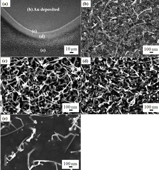
Figure 1. (a) FE-SEM images of Ga2O3 nanowires grown on a 3 nm thick gold catalyst layer. Images (b)-(e) are magnified images of the areas indicated in image (a).

Figure 2. AFM images of gold particles annealed at 750˚C under oxygen pressure of 0.1 Pa before nanowire growth. The thickness of deposited gold was 3 nm for (a)-(d) and 1 nm for (e). Images (a)-(d) were measured at approximately 150 μm, 190 μm, 210 μm, and 235 μm away from the center of gold layer on the substrate in turn, respectively. Image (e) shows an area near the center of the gold film. The average size of gold particles is as follows: (a) 79 nm; (b) 48 nm; (c) 24 nm; (d) 19 nm; and (e) 18 nm.
Figure 3 shows FE-SEM images of Ga2O3 nanowires grown on a 1 nm thick gold catalyst at 700˚C, 750˚C, 800˚C, and 850˚C. As shown in the insets of Figure 3, growth of nanowires with uniform length and width was confirmed in the wide area where gold was sputtered. As seen in the images, the density of nanowires increased with increasing growth temperature. Judging from the similar morphologies in Figures 2(d) and (e), it is supposed that nanowires of phase 3 grew in the vicinity of the area shown in Figure 2(d). Thus, the thickness of the gold catalyst was a crucial parameter responsible for the observed Ga2O3 nanowire morphologies.
In order to investigate the crystal structures of the Ga2O3 nanowires, transmission electron microscopy (TEM) analysis was performed. The TEM images, selective area electron diffraction (SAED), and distribution of diameters are shown in Figure 4. As shown in Figure 4(c), the diameters of nanowires were distributed in the range of 6 - 27 nm. The lattice spacing perpendicular to the nanowires growth direction was directly estimated from TEM images. Lattice spacing varied from 0.56 to 0.59 nm with an average value of 0.578 nm, which was close to the spacing of (001) lattice planes (0.565 nm) of monoclinic β-Ga2O3 as reported in the X-ray diffraction pattern JCPDS 41-1103 [14]. The SAED pattern showed fringes and bright spots (see the inset of Figure 4(a), indicating that the nanowires consist of a single crystalline structure at the core and a surrounding polycrystalline structure.

Figure 3. FE-SEM images of Ga2O3 nanowires grown on 1 nm thick gold catalyst at growth temperatures of (a) 700˚C; (b) 750˚C; (c) 800˚C; and (d) 850˚C. The inset shows FESEM images scanned in wide range.

Figure 4. (a) TEM image of Ga2O3 nanowires. Inset is SAED image; (b) Enlarged TEM image of a single Ga2O3 nanowire; (c) Diameter distribution as obtained from TEM images.
Figure 5 shows the CL spectra of Ga2O3 nanowires as-grown at 700˚C - 850˚C. In the spectrum of nanowires grown at 850˚C there were four emission bands with peaks at 359, 411, 512 and weak—696 nm, which were characterized as UV, blue, green, and red emissions, respectively [15]. Since UV emission peaks are generally attributed to an intrinsic recombination of an electron (or hole) and a self-trapped hole (or electron) [16], the intensity of the other CL peaks were normalized to the UV emission peak. The CL spectra for all samples were well fitted by four Gaussian curves, corresponding to UV, blue, green, and red emissions, respectively. As shown in Figure 6, the relative intensities of blue, green, and red bands were found to decrease with an increasing growth temperature. The blue emission was attributed to a recombination of holes at acceptor sites and electrons tunnel-transferred from donor clusters, as suggested by Binet et al. [17]. Green emission is possibly associated with self-trapped or bound excitons [18]; however, its mechanism has not been clarified yet. Red luminescence was first reported in N-doped Ga2O3 nanowires by Song et. al. [19]. They explained that the red emission originated from the recombination of electrons trapped by donors (oxygen vacancies) and holes trapped by acceptor sites. In Ga2O3, donor and acceptor sites would be formed by oxygen vacancies (VO) and paired gallium and oxygen vacancies (VO, VGa), respectively [17]. In this study, it was expected that a number of O vacancies and (VO, VGa) pairs were included in the nanowires because they were synthesized in a nonequilibrium process under a low oxygen pressure of 0.1 Pa. In order to investigate the contribution to CL by oxygen vacancies, Ga2O3 nanowires were annealed at 600˚C for 1 h in air. Since the nanowires were annealed at a lower temperature than their growth temperature, there were no significant differences in their morphology after annealing. The CL spectra of Ga2O3 nanowires grown at 850˚C, before and after annealing are shown in Figure 5. As shown in Figure 6, the relative intensities of blue, green, and red emissions decreased in all samples after annealing in air. This result suggests that the blue, green, and red bands were associated with the energy levels of oxygen vacancies. As evaluated from TEM images, the nanowires showed a larger lattice constant (0.578 nm) than the value reported in X-ray diffraction (0.565 nm), which may be evidence that oxygen vacancies are contained in the nanowires. The decrease in blue, green, and red emission peaks after thermal annealing was probably due to the compensation of oxygen vacancies. Thus, thermal annealing was effective in obtaining enhanced UV emission for optical applications.

Figure 5. CL spectra measured for Ga2O3 nanowires, as deposited at various temperatures in the range 700˚C to 850˚C, and nanowires annealed at 600˚C after deposition at 850˚C. The dotted line shows the fitting curve for four Gaussian curves (UV, blue, green, and red).

Figure 6. Growth temperature dependence of CL relative intensities for blue, green, and red emissions. Blank and filled symbols indicate as deposited and annealed Ga2O3 nanowires, respectively.
4. Conclusion
Ga2O3 nanowires were fabricated by pulsed laser deposition on a gold catalyst. In the VLS process, gold thickness was a crucial parameter in deciding nanowire morphology. On 1 nm thick gold, homogeneous nanowire growth was confirmed in the range growth temperatures of 700˚C - 850˚C. TEM and SAED measurements showed that the nanowires consisted of polycrystalline phases. UV, blue, green, and red CL peaks were observed, as reported in previous studies. As the growth temperature increased, the relative intensities of blue, green, and red emissions were found to decrease. Annealing treatment was also effective for decreasing the deficiency-related blue, green, and red emissions.
5. Acknowledgements
This work was supported by the Grant-in-Aid for the Global COE Program “Secure-Life Electronics” from the Ministry of Education, Culture, Sports, Science and Technology (MEXT), Japan. Part of this work was conducted at the Center for Nano Lithography & Analysis of The University of Tokyo, supported by MEXT, Japan.
REFERENCES
- T. Yanagida, K. Nagashima, H. Tanaka and T. Kawai, “Mechanism of Catalyst Diffusion on Magnesium Oxide Nanowire Growth,” Applied Physics Letters, Vol. 91, No. 6, 2007, Article No. 061502. doi:10.1063/1.2768202
- J. Maeng, W. Park, M. Choe, G. Jo, Y. H. Kahng and T. Lee, “Transient Drain Current Characteristics of ZnO Nanowire Field Effect Transistors,” Applied Physics Letters, Vol. 95, No. 12, 2009, Article No. 123101. doi:10.1063/1.3232203
- A. Qurashi, E. M. El-Maghraby, T. Yamazaki and T. Kikuta, “Catalyst Supported Growth of In2O3 Nanostructures and Their Hydrogen Gas Sensing Properties,” Sensors and Actuators B, Vol. 147, No. 1, 2010, pp. 48-54. doi:10.1016/j.snb.2010.03.024
- K. Nagashima, T. Yanagida, A. Klamchuen, M. Kanai, K. Oka, S. Seki and T. Kawai, “Interfacial Efect on Metal/ Oxide Nanowire Junctions,” Applied Physics Letters, Vol. 96, No. 7, 2010, Article No. 073110. doi:10.1063/1.3318257
- K. Matsuzaki, H. Yanagi, T. Kamiya, H. Hiramatsu, K. Nomura, M. Hirano and H. Hosono, “Field-Induced Current Modulation in Epitaxial Film of Deep-Ultraviolet Transparent Oxide Semiconductor Ga2O3,” Applied Physics Letters, Vol. 88, No. 9, 2006, Article No. 092106. doi:10.1063/1.2179373
- N. D. Cuong, Y. W. Park and S. G. Yoon, “Microstructural and Electrical Properties of Ga2O3 Nanowires Grown at Various Temperatures by Vapor-Liquid-Solid Technique,” Sensors and Actuators B, Vol. 140, No. 1 2009, pp. 240-244. doi:10.1016/j.snb.2009.04.020
- M. Orita, H. Ohta, M. Hirano and H. Hosono, “DeepUltraviolet Transparent Conductive β-Ga2O3 Thin Films,” Applied Physics Letters, Vol. 77, No. 25, 2000, Article No. 4166. doi:10.1063/1.1330559
- H. Z. Zhang, Y. C. Kong, Y. Z. Wang, X. Du, Z. G. Bai, J. J. Wang, D. P. Yu, Y. Ding, Q. L. Hang and S. Q. Feng, “Ga2O3 Nanowires Prepared by Physical Evaporation,” Solid State Communications, Vol. 109, No. 11, 1999, pp. 677-682. doi:10.1016/S0038-1098(99)00015-0
- W. Q. Han, P. Kohler-Redlich, F. Ernst and M. Rühle, “Growth and Microstructure of Ga2O3 Nanorods,” Solid State Communications, Vol. 115, No. 10, 2000, pp. 527-529. doi:10.1016/S0038-1098(00)00238-6
- H. J. Chun, Y. S. Choi, S. Y. Bae, H. W. Seo, S. J. Hong, J. Park and H. Yang, “Controlled Structure of Gallium Oxide Nanowires,” Journal of Physical Chemistry B, Vol. 107, No. 34, 2003, pp. 9042-9046. doi:10.1021/jp034728o
- H. W. Kim and N. H. Kim, “Synthesis of β-Ga2O3 Nanowires by an MOCVD Approach,” Applied Physics A, Vol. 81, No. 4, 2005, pp. 763-765. doi:10.1007/s00339-004-2982-6
- M. Orita, H. Hiramatsu, H. Ohta, M. Hirano and H. Hosono, “Preparation of Highly Conductive, Deep Ultraviolet Transparent β-Ga2O3 Thin Film at Low Deposition Temperatures,” Thin Solid Films, Vol. 411, No. 1, 2002, pp. 134-139. doi:10.1016/S0040-6090(02)00202-X,
- H. Hayashi, R. Huang, H. Ikeno, F. Oba, S. Yoshioka, I. Tanaka and S. Sonoda, “Room Temperature Ferromagnetism in Mn-doped γ-Ga2O3 with Spinel Structure,” Applied Physics Letters, Vol. 89, No. 18, 2006. Article No. 181903. doi:10.1063/1.2369541
- F. Shi, S. Zhang and C. Xue, “Influence of Annealing Time on Microstructure of One-Dimensional Ga2O3 Nanorods,” Journal of Alloys and Compounds, Vol. 498, No. 1, 2010, pp. 77-80. doi:10.1016/j.jallcom.2010.03.106
- J. Zhang, B. Li, C. Xia, G. Pei, Q. Deng, Z. Yang, W. Xu, H. Shi, F. Wu, Y. Wu and J. Xu, “Growth and Spectral Characterization of β-Ga2O3 Single Crystals,” Journal of Physics and Chemistry of Solids, Vol. 67, No. 12, 2006, pp. 2448-2451. doi:10.1016/j.jpcs.2006.06.025
- T. Harwig, F. Kellendonk and S. Slappendel, “The Ultraviolet Luminescence of β-Galliumsesquioxide,” Journal of Physics and Chemistry of Solids, Vol. 39, No. 6, 1977, pp. 675-680. doi:10.1016/0022-3697(78)90183-X
- L. Binet and D. Gourier, “Origin of the Blue Luminescence of β-Ga2O3,” Journal of Physics and Chemistry of Solids,, Vol. 59, No. 8, 1998, pp. 1241-1249. doi:10.1016/S0022-3697(98)00047-X
- E. G. Víllora, M. Yamaga, T. Inoue, S. Yabasi, Y. Masui, T. Sugawara and T. Fukuda, “Optical Spectroscopy Study on β-Ga2O3,” Japanese Journal of Applied Physics, Vol. 41, No. 6A, 2002, pp. L622-L625. doi:10.1143/JJAP.41.L622
- Y. P. Song, H. Z. Zhang, C. Lin, Y. W. Zhu, G. H. Li, F. H. Yang and D. P. Yu, “Luminescence Emission Originating from Nitrogen Doping of β-Ga2O3 Nanowires,” Physical Review B, Vol. 69, No. 7, 2004, Article No. 075304. doi: 10.1103/PhysRevB.69.075304.
NOTES
*Corresponding author.