Journal of Crystallization Process and Technology
Vol.1 No.2(2011), Article ID:6548,5 pages DOI:10.4236/jcpt.2011.12003
A New Method for Research of Grown-In Microdefects in Dislocation-Free Silicon Single Crystals
![]()
Department of Programming & Information Technology, Classic Private University, Zaporozhye, Ukraine.
E-mail: v.i.talanin@mail.ru
Received May 16, 2011; revised June 20, 2011; accepted June 28, 2011.
Keywords: Silicon, Grown-In Microdefects, Precipitate, Vacancy Microvoid, Interstitial Dislocation Loop
ABSTRACT
As a virtual experimental device for analysis and calculation of grown-in microdefects formation in undoped silicon dislocation-free single crystals the software is proposed. The software is built on the basis on diffusion model of formation, growth and coalescence of grown-in microdefects. Diffusion model describes kinetics of defect structure changes during cooling after growth on crystallization temperature to room temperature. The software allows the use of personal computer to investigate the defect structure of dislocation-free silicon single crystals with a diameter on 30 mm to 400 mm grown by floating-zone and Czochralski methods.
1. Introduction
A vast majority of modern microelectronic and nanoelectronic devices are built on the monocrystalline silicon substrates produced from the crystals grown by the Czochralski (CZ) process and the float-zone (FZ) process. Many of the advances in integrated-circuit (IC) manufacturing achieved in recent years would not have been possible without parallel advances in silicon-crystal quality and defect engineering. These studies are now approaching values that will allow the silicon starting material to be used in the production of critical component dimensions below 18 nm [1].
Silicon crystals grown by the Czochralski process and floating zone method typically contain many structural imperfections termed grown-in microdefects. Grown-in microdefects degrade the electronic properties of microdevices fabricated on silicon wafers. Optimizing the number and size of grown-in microdefects is crucial to improving processing yield of microelectronic devices. The problem of defect formation in dislocation-free silicon single crystals during their growth is a fundamental problem of physics and chemistry of silicon. This problem is key to solving other complex problems in physics, chemistry, materials science and engineering applications of silicon crystals.
Currently, as a result of many studies of dislocationfree silicon single crystals obtained various experimental data concerning the formation and interaction of point defects, has accumulated vast experience in growing perfect crystals [1,2]. It was established that grown-in microdefects are precipitates of impurities, interstitial dislocation loops and vacancy microvoids [3,4]. However, experimental studies require large material and time costs, while theoretical studies are carried out for single crystals with selected fixed parameters of their growth [5,6]. Consequently, it is necessary to develop a new method for studying the defect structure of silicon without these drawbacks. This method allows to simulate a real experiment by the software.
The aim of this work is to develop a new method of research of grown-in microdefects in dislocation-free silicon single crystals, based on IT-technologies.
2. Experimental Technique
Physical model of software system based on the diffusion model formation of microdefects. In turn, the diffusion model of formation microdefects is based on the following experimental data: 1) The recombination of intrinsic point defects at high temperatures can be neglected [7]; 2) Background carbon and oxygen impurities are involved in the defect formation as nucleation centers [3]; 3) The decay of the supersaturated solid solution of point defects when the crystal is cooled from the crystallization temperature occurs in two independent ways (branches): vacancy and interstitial [2]; 4) The basis of the formation defect is the elastic interaction between the impurities and intrinsic point defects [8]; 5) When the crystal is cooled at temperatures below 1150˚C, depending on the thermal growth conditions, vacancy microvoids or interstitial dislocation loops are formed [3]; 6) The vacancy microvoids or interstitial dislocation loops are formed due to the coagulation (vacancy microvoids and interstitial dislocation loops) and deformation (interstitial dislocation loops) effects [9]; 7) The formation of vacancy microvoids or interstitial dislocation loops controlled growth parameter , where
  is the crystal growth rate and
  is the axial temperature gradient (vacancy microvoids are formed at
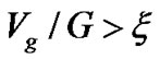 , and interstitial dislocation loops arise at
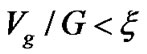 ) [2,10].
Diffusion model of the formation of grown-in microdefects assumes that the defects formation in dislocation-free silicon single crystals upon cooling occurs in three stages: 1) The formation of impurity agglomerates near the crystallization front [8], 2) Formation, growth and coalescence of impurity precipitates upon cooling from the crystallization temperature [6]; 3) Formation of vacancy microvoids or interstitial dislocation loops (depending on the growth of the parameter  at temperature
 ˚C, where
  is the melting temperature) [9].
In the diffusion model of formation grown-in microdefects all the parameters of precipitates, vacancy microvoids and interstitial dislocation loops are determined through the thermal conditions of growth. Therefore, definition the type of defect structure and calculation of the formation of microdefects is conducted depending on the values of crystal growth rate, temperature gradients and cooling rate of the crystal.
Determination of the type of the defect structure carried based on the standard pictures of the selective etching of grown-in microdefects depending on the crystal growth rate. In Figure 1 shows such distribution for a crystal with a diameter of 50 mm grown by the Czochralski [2]. V-shaped distribution of precipitates of oxygen and carbon (or OSF-ring in the plane (111) after thermal treatment of the crystal, where OSF is the oxidation stacking fault) determined of the growth parameter . If
. If 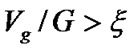 precipitates observed inside and above the V-shaped distribution and when
 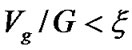 observed precipitates and interstitial dislocation loops [2].
Increasing the diameter of the crystal leads to a change in temperature conditions of growth and dislocation-free
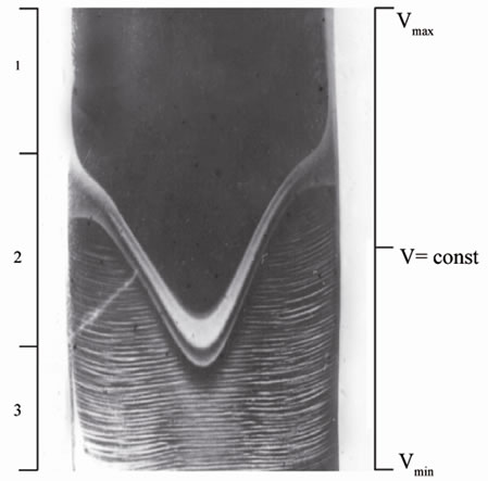
Figure 1. Standard pattern of distribution of grown-in microdefects in dislocation-free silicon single crystals grown by the Czochralski method with a variable rate of growth (Vmin = 0.5 mm/min; Vmax = 3.0 mm/min; diametr is the 50 mm).
crystal growth in a limited range of rates [11]. In this case the conditions of existence only of the V-shaped distribution of precipitates are executed. Inside the V-shaped distribution of precipitates exist precipitates and vacancy microvoids. The formation of vacancy microvoids occurs when the crystal diameter is the greater than 80 mm [12]. Outside the V-shaped distribution of precipitates are formed precipitates and interstitial dislocation loops.
V-shaped distribution of precipitates depends on the parabolic radial distribution of the axial temperature gradient: , where
  is the radius of the crystal;
  is the current coordinate in the range from 0 to
 ,
,  is the axial temperature gradient in the center of the crystal,
  is the axial temperature gradient at the edge of the crystal. In the case of W-shaped distribution of precipitates [13] dependence of
  can be approximated by two parabolic distributions.
To calculate the formation of grown-in microdefects been used two mathematical approaches: the analytical calculations (I) and approximate calculations (II). In the case of (I) it is a solution of differential equations of the dissociative diffusion [12]. In the case of (II) solution is sought in the form of systems of interconnected discrete differential equations of the quasi-chemical reactions to describe the initial stages of nucleation of new phases, and a similar system of continual differential equations of the Fokker-Planck equation [8].
3. The Structure of the Software System
The object of research is the process of defect formation during crystal growth. Mathematical models of the formation of grown-in microdefects give the equivalent of an object, which in mathematical form reflects the most important of its properties. Electronic equivalent of an object for direct test on the computer are programs that converted the mathematical models and algorithms to the available computer language (C++). The program is written high-level language programming in C++ compiler Borland C++ Builder. Program complex consists of two consecutive parts: 1) The unit determination the type of defect structure and 2) The unit of calculation and graphs (Figure 2).
At the stage of determining the type of the structure defect of software system works as follows. Initially is the choice of method of growing dislocation-free silicon single crystals (Czochralski method or the floating-zone method) and then is the choice of certain diameter of the crystal. The ratio of  theoretically and experimentally determined in a certain range of values (0.06 mm2 / K·min ≤
 ≤ 0,3 mm2 / K·min). Therefore, we choose the certain value
  for the calculation.
For a given diameter in a certain range of values are selected: the value of the axial temperature gradient in the center of the crystal ( ) and the value of the minimum (
 ) and maximum (
 ) crystal growth rate. These values are determined from the analysis of experimental and theoretical data for different diameters of the crystal. Then produced choice of the axial temperature gradient at the edge of the crystal (
 ) in the range
  = 1.0 ... 2.5.
The reliability and accuracy of the computational experiments can be experimentally verified by means of selective etching crystal of the plane which passes through the center of the crystal and parallel to the direction of growth. In case of deviations can by using of the selection of parameters  achieve full compliance with theoretical and experimental data. In addition, this technique avoids the difficulties of experimental
Figure 2. Original form of software system.
determination of the  and
and , especially for large diameter crystals.
At the last stage of determining the type of defect structure on the resulting dependence of the critical growth rate  is imposed value of real crystal growth rate
  (Figures 1 and 3). This procedure allows determining the type of defect structure of a real crystal. Depending on the position of the line
  relative to the curve
 may be three areas of the defect structure. Calculation of these areas produced the block of calculation and graphs (Figure 4).
The first area of the calculation is characterized by high rates of crystal growth, when the above V-shaped distribution of precipitates formed only vacancy microvoids and precipitates. The second area of calculation is characterized by the average growth rate of the crystal, when a ring of precipitate in the plane perpendicular to the direction of growth crystal is formed. In this case inside the ring are formed precipitates and vacancy microvoids, outside the ring are formed precipitates and interstitial dislocation loops. The third area of calculation is characterized by low rates of crystal growth, when the below V-shaped distribution of precipitates are formed precipitates and interstitial dislocation loops (Figure 3).
Calculation of the precipitates is carried out within the classical theory of nucleation, growth and coalescence of precipitates by means of the analytical and approximatecalculations. Critical radius of precipitates, the distribution of precipitates in size, change in the average size of precipitates during the cooling of the crystal, and other parameters of the precipitation of carbon and oxygen are determined (Figure 4). Mathematical models and calculation parameters are given in [6,8,9,12].
When calculating the vacancy microvoids initially are tested of conditions their formation, since vacancy microvoids are not formed at a cooling rate of the crystal
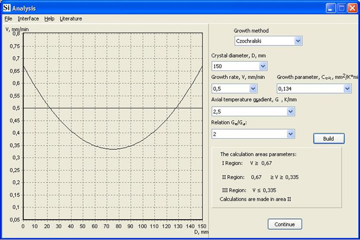
Figure 3. Shape analysis of the defect structure.
 [14] and in crystals with a diameter less than 80 mm [12]. Calculation of the vacancy microvoids and interstitial dislocation loops to determines for each of these types of defects such parameters as the critical radii and the concentrations [9].
4. Conclusions
The program complex is the first experience of a virtual experimental device for research the real structure of dislocation-free silicon single crystals. Currently, it can be used for the analysis and calculation of the defect structure of undoped single-crystal silicon. Substitution of experimental researches of structure of adequate theoretical studies using the program complex suggests that the complex is a new virtual experimental device. Since the technique of application software is original, it is the new experimental techniques.
Disadvantages software system are determined deficiencies of the diffusion model of formation grown-in microdefects. These include: 1) One-dimensional model; 2) Failure to account for the width of the V-shaped distribution of precipitates; 3) Uncertainty in determining of thermal conditions of growth; 4) The error of approximate numerical methods.
The software complex performs imitation of a real experiment and with the maximum precision reproduces the thermal characteristics of silicon single crystal growing. The software complex allows to determine the thermal conditions of crystal growth, to predict and control the defect structure of the crystal. Calculations formation of grown-in microdefects are in good agreement with the experimental results of research.
Approach to the analysis and calculation of formation grown-in microdefects has an important advantage in simplicity, accessibility and sufficient adequacy of mathematical modeling in comparison with other methods. For its implementation does not require supercom-puters, and can effectively use the experimental data, experience and intuition of physicists, materials scientists and
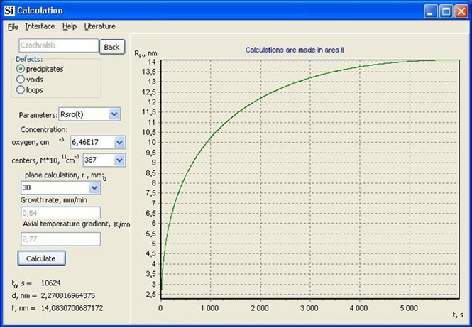
Figure 4. Form of calculation of the defect structure.
technologists for the analytical calculation and design of the defect structure. The program complex is easy to implement on a personal computer in technology and research practices.
5. References
[1] E. Tomzig, “Status of growing large Si crystals (300 mm) and outlook to larger diameter crystals (450 mm). Aspects of crystal growth, defects and impurities,” In: B. O. Kolbesen, C. Claeys, L. Fabry and F. Tardif, Eds., Crystalline defects and contamination: their impact and control in device manufacturing IV, Electrochemical Society, Inc., Pennington, 2005, pp. 3-15.
[2] V. I. Talanin and I. E. Talanin, “Formation of grown-In microdefects in dislocation-free silicon monocrystals,” In: T. B. Elliot, Ed., New research on semiconductors, Nova Science Publishers, Inc., New York, 2006, pp. 31- 67.
[3] V. I. Talanin and I. E. Talanin, “Mechanism of formation and physical classification of the grown-in microdefects in semiconductor silicon,” Defect & Diffusion Forum, Vol. 230-232, No. 1, 2004, pp. 177-198. doi:10.4028/www.scientific.net/DDF.230-232.177
[4] M. S. Kulkarni, J. C. Holzer and L. W. Ferry, “The agglomeration dynamics of self-interstitials in growing Czochralski silicon crystals,” Journal of Crystal Growth, Vol. 284, No. 3-4, 2005, pp. 353-368. doi:10.4028/www.scientific.net/DDF.230-232.177
[5] M. S. Kulkarni, V. Voronkov and R. Falster, “Quantification of defect dynamics in unsteady state and steadystate Czochralski growth of monocrystalline silicon,” Journal of The Electrochemical Society, Vol. 151, No. 5, 2004, pp. G663-G669. doi:10.4028/www.scientific.net/DDF.230-232.177
[6] V. I. Talanin and I. E. Talanin, “Kinetics model of growth and coalescence of oxygen and carbon precipitates during cooling of as-grown silicon crystals,” Physics of the Solid State, Vol. 53. No. 1, 2011, pp. 119-126. doi:10.4028/www.scientific.net/DDF.230-232.177
[7] V. I. Talanin and I. E. Talanin, “On the recombinetion of intrinsic point defects in dislocation-free silicon single crystals,” Physics of the Solid State, Vol. 49, No. 3, 2007, pp. 467-470. doi:10.1134/S1063783407030134
[8] V. I. Talanin and I. E. Talanin, “Kinetics of high-temperature precipitation in dislocation-free silicon single crystals,” Physics of the Solid State, Vol. 52, No. 10, 2010, pp. 2063-2068. doi:10.1134/S1063783410100094
[9] V. I. Talanin and I. E. Talanin, “Kinetis of formation of vacancy microvoids and interstitial dislocation loops in dislocation-free silicon crystals,” Physics of the Solid State, Vol. 52, No. 9, 2010, pp. 1880-1886. doi:10.1134/S1063783410100094
[10] V. V. Voronkov, “Mechanism of swirl defects formation in silicon,” Journal of Crystal Growth, Vol. 59, No. 3, 1982, pp. 625-642.doi:10.1016/0022-0248(82)90386-4
[11] W. Von Ammon, E.Dornberger and P.O.Hansson, “Bulk properties of very large diameter silicon single crystal,” Journal of Crystal Growth, Vol. 198-199, No. 1-4, 1999, pp. 390-398. doi:10.1016/S0022-0248(98)01140-3
[12] V. I. Talanin and I. E. Talanin, “Modeling of defect formation processes in dislocation-free silicon single crystals,” Crystallography Reports, Vol. 55. No. 4, 2010, pp. 632-637. doi:10.1134/S1063774510040164
[13] A. Natsume, N. Inoue, K. Tanahashi and A. Mori, “Dependence of temperature gradient on growth rate in CZ silicon,” Journal of Crystal Growth, Vol. 225, 2001, pp. 221-224.doi:10.1016/S0022-0248(01)00837-5
[14] K. Nakamura, T. Saishoji and J. Tomioka, “Grown-in defects in silicon crystals,” Journal of Crystal Growth, Vol. 237-239, No. 10, 2002, pp. 1678-1684.doi:10.1016/S0022-0248(01)02323-5